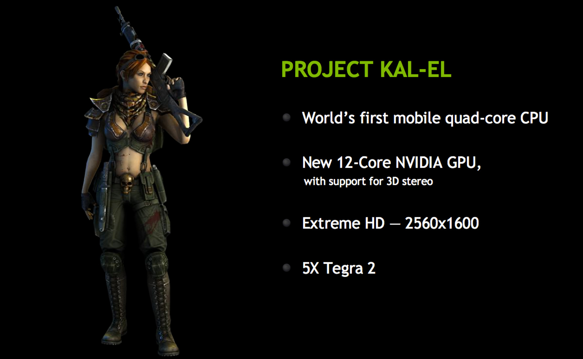


goplayer361 发表于 2011-2-16 14:33
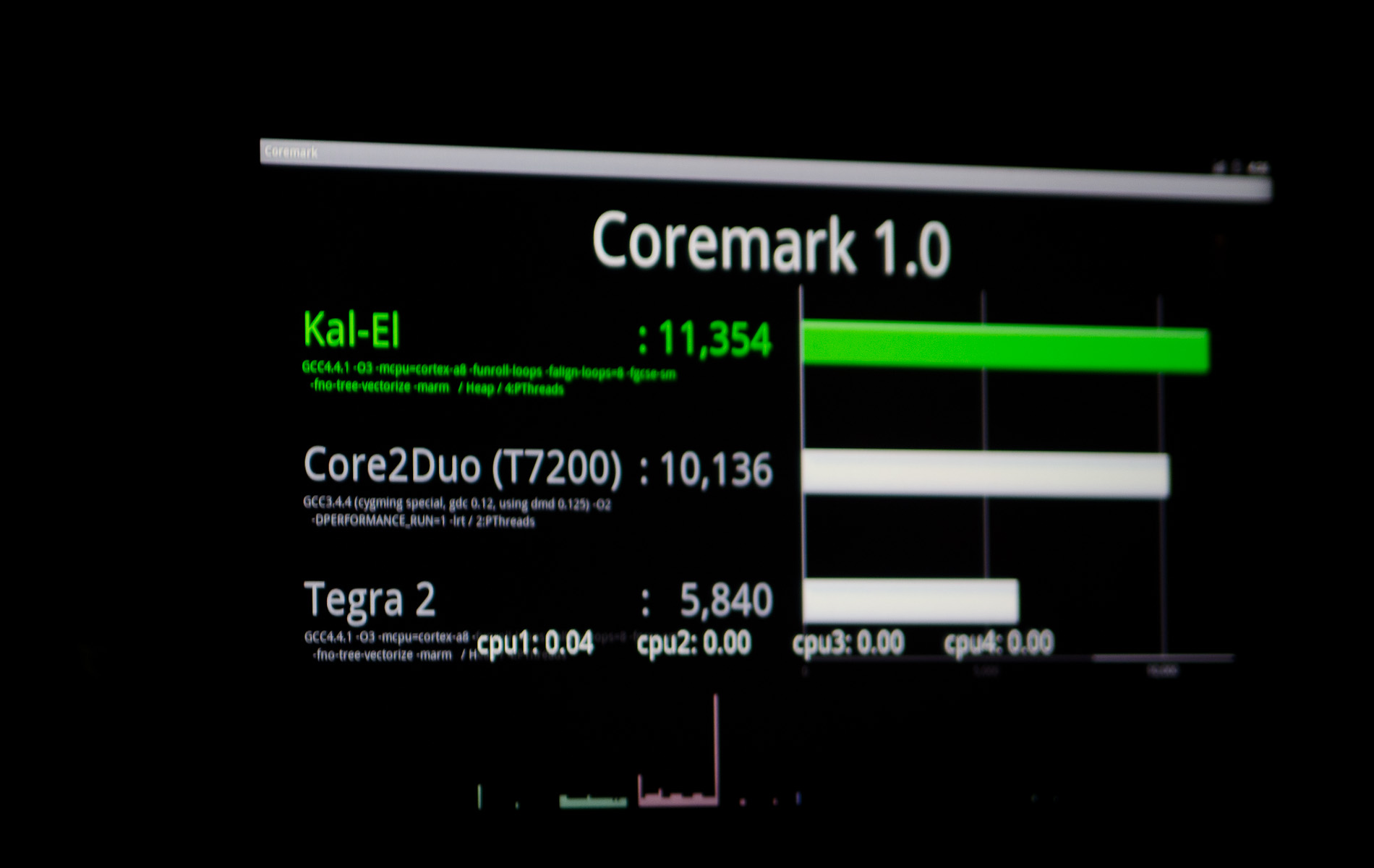
又开始指导性测试了?这数据。。。啧啧
 这点我感觉其他商家还是不够给力啊
goplayer361 发表于 2011-2-16 14:39
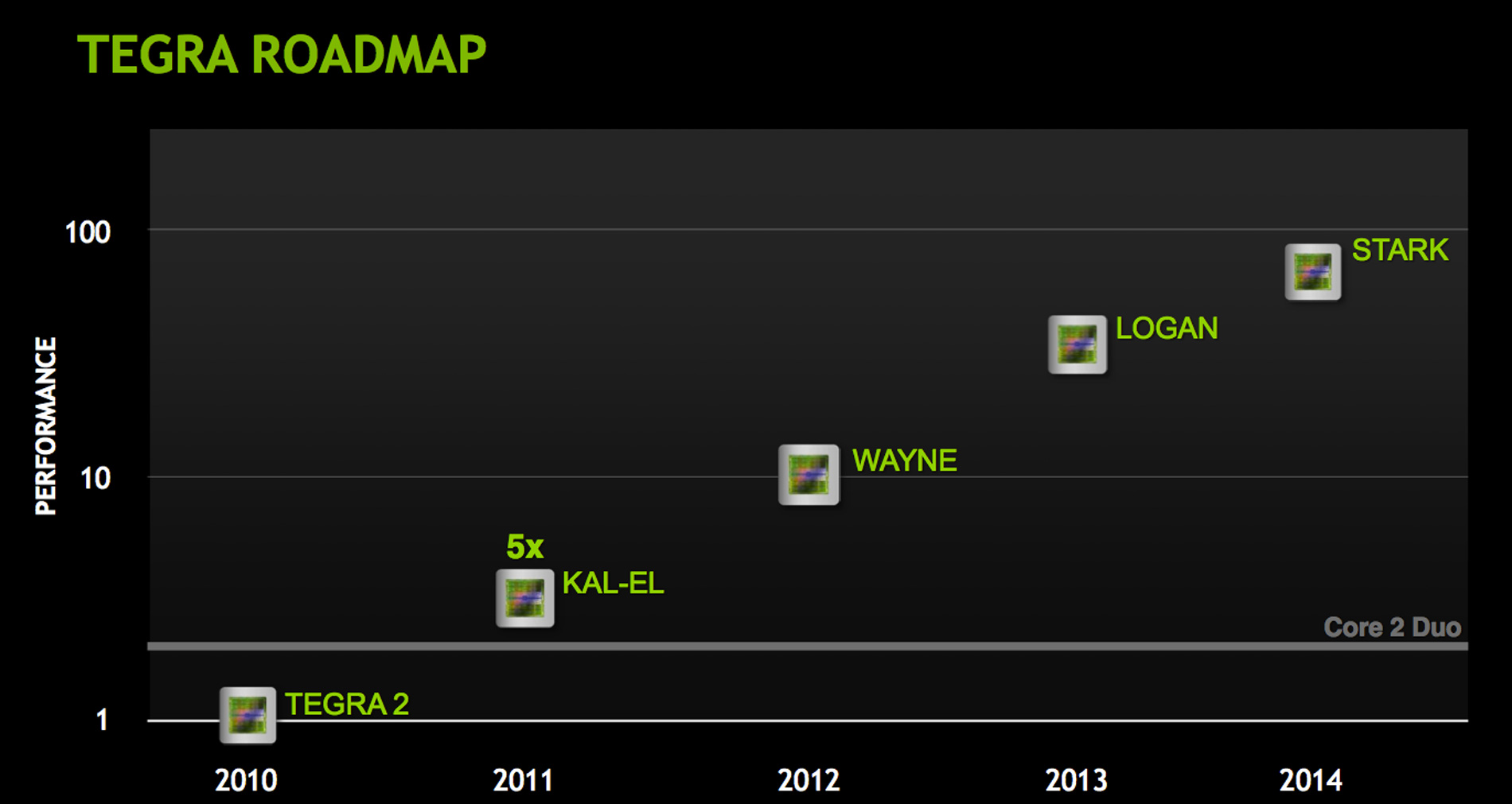
对nv的图表结果我印象最深的就是截一段再比较 结果看上去非常夸张的差距其实就是那么一点点

Heitai 发表于 2011-2-16 23:37
高通的4核是28nm的吧?

 反正INTEL以后日子不会好过了
Edison 发表于 2011-2-16 14:41
这个问题你自己如果不偏颇的话,大可以找出许多其他厂商类似的官方非零原点坐标对比图表。
 我没记错的话。dual cor尺寸从11*11到14*14的。很奇怪Tegra的PMIC是谁家的?
66666 发表于 2011-2-18 16:52
回复 kyrome 的帖子
tegra3八月份出货,索爱这个明年这时候能看到实物就不错了


eoc 发表于 2011-2-22 02:10
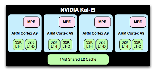
硬解码方面,NV相比三星落后了。S5PC110已经可以硬解10REF FRAME以上的HIGH PROFILE H.264视频了。NV的Tegr ...
Edison 发表于 2011-2-16 23:42
高通的是 Cortex A-15,不过时间依然落后同等级的 NVIDIA Tegra 4 一年。
| 欢迎光临 POPPUR爱换 (https://we.poppur.com/) | Powered by Discuz! X3.4 |

