原帖由 hopetoknow2 于 2006-7-5 15:50 发表
那个就是65nm die, 和AMD公布的一致, 自己看去


原帖由 电脑是工具 于 2006-5-17 10:40 发表
K8L明年上半年上市。
原帖由 黑真PIG 于 2006-5-17 10:52 发表
虽说"2007 will be a fight after all"
可Am2出了样品, 唱了快一年了还没有动静, 你信K8L 2007上半年上市?
原帖由 电脑是工具 于 2006-5-17 11:08 发表
fans所以是fans,就是因为脑子坏掉了,自己都不知道自己在说什么。
AM2没动静?昨天刚发布了低功耗的AM2,一周后发布其他的AM2,这个月开始陆续供货。
AM2相比规划,延迟了大概2个月。65NM CD也延迟了一个 ...
原帖由 ppzhong 于 2006-5-17 11:23 发表
这种CPU,4核的估计真的没2008都出不来,纸上谈兵,谁都会啊,K8老了。。。。。。。。。。AMD的65纳秒看都没看到,别跟我说AMD用90NS做个4核心U。。。。。。。
原帖由 Edison 于 2006-5-17 11:31 发表
怎么说K8L没有图片呢?我在贴中已经给出了K8L管芯的图片。
此外,你们看到的消息发布并不等于说消息发布的时候才确定cpu设计,大部分情况下都是在此前一年就已经确定了,只不过是基于各种原因一直处于保密状态 ...
原帖由 黑真PIG 于 2006-5-17 11:32 发表
虽然这样说, 但4核, 还是2008年比较相信 :lol:
原帖由 Edison 于 2006-5-17 11:34 发表
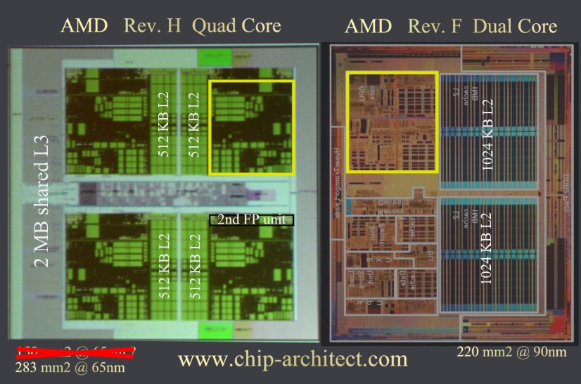
四内核的K8L die size只有150平方毫米,die size只是比双内核的Conroe大10平方毫米,明年推出的机会远远大于2008年。
原帖由 黑真PIG 于 2006-5-17 11:40 发表
对我来说4核心还是梦想中的东西 :a)
原帖由 babystudio 于 2006-5-17 11:44 发表
到那个时候Intel和AMD目前的处境相信会对调的
原帖由 黑真PIG 于 2006-5-17 11:49 发表
这个是服务器用的...
不是民用的:sweatingbullets:
原帖由 Edison 于 2006-5-17 11:52 发表
他们都是民用的,不是军用的。
150mm^2的die size非常不错,90nm Rev.F的die size是220mm^2,K8L的die size只有 90nm Rev.F dual core K8的68%左右。
换句话说,K8L制造成本是目前90nm双内核K8的68%。
原帖由 GZboy 于 2006-5-17 11:22 发表
全文看完~结论——新一 代硅渣:shifty:

原帖由 hbdavidlee 于 2006-5-17 07:38 PM 发表
就目前的发展前景来看,AMD的市场很不容乐观.....65NM工艺自己都搞不定还要靠IBM的技术,这只能说明AMD的技术匮乏,就技术层面AMD绝对和intel没的比,至于A64这种借鉴alpha处理器的垃圾技术只能说是恰巧撞上p4 e的 ...
原帖由 oliverli 于 2006-5-18 00:52 发表
看来针对扣肉的YY正式宣布结束了
原帖由 黑真PIG 于 2006-5-17 11:18 发表
AMD从发布样品, 发布接口等等, 用了多久? 3个月前就有ES版了, 如今才发布. hoho
这种发布也是学ATI, 口头发布. 等一段时间才能铺货.
K8L目前只有文字资料, 连个图片都没有, 你说什么时候? :shifty:
而 ...
原帖由 hammerking 于 2006-5-20 23:44 发表
如果65nm工艺下qc的k8L核心面积真的是只有150mm^2,那dc核心面积肯定在100mm^2以内,amd的产能问题会得到很大程度上的解决,不过不知道amd怎么做到的,即使per core L2减少到512k,考虑到四个核心,且核心有重大改 ...
原帖由 hammerking 于 2006-5-20 23:44 发表
如果65nm工艺下qc的k8L核心面积真的是只有150mm^2,那dc核心面积肯定在100mm^2以内,amd的产能问题会得到很大程度上的解决,不过不知道amd怎么做到的,即使per core L2减少到512k,考虑到四个核心,且核心有重大改 ...
原帖由 hammerking 于 2006-5-21 00:17 发表
按你这么说还是比150mm^2大得多啊。
原帖由 GZboy 于 2006-5-17 13:15 发表
K8L的对手会是CORE2吗?:shifty:
是CORE2的后续版本,原生4核的
查一下INTEL 07年的时间表再回来说吧。-_-
原帖由 shu0202 于 2006-7-5 09:17 发表
多核心AMD居然比Intel跑得更快,真让Intel挠心啊。
原帖由 hammerking 于 2006-5-20 23:44 发表
如果65nm工艺下qc的k8L核心面积真的是只有150mm^2,那dc核心面积肯定在100mm^2以内,amd的产能问题会得到很大程度上的解决,不过不知道amd怎么做到的,即使per core L2减少到512k,考虑到四个核心,且核心有重大改 ...
原帖由 hammerking 于 2006-7-5 12:16 发表
kao,这么老的帖子又挖出来的,我自己也不大相信qc k8L的die只有150mm^2,chip-architech的说法,仅供参考。至于核心改进么 。#走着瞧B)
原帖由 hammerking 于 2006-5-20 23:19 发表
呵呵,如果真是这么sb,那么amd的工程师且不是白痴?应该聘请你去设计cpu,少来这胡说八道了。
amd目前不用share L2的最大原因是k8的L1,L2结构不适合share L2,,k8的L1中有的数据,L2中不会有,如果共享L2,会 ...
原帖由 hammerking 于 2006-7-5 15:16 发表
唉,懒得跟你说了,你所谓的论据全部是自己 的臆测,自己慢慢yy把。(_(
原帖由 hopetoknow2 于 2006-7-5 12:23 发表
150mm2简直是乱来。
看看真正使用65nm核心, 合理构造出来的K8L图吧:
3倍于65nm的K8单核
换算下来K8L (QC)其面积几乎>310mm2
远远超过Conroe 4M的140mm2两倍还多。
原帖由 单晶硅传奇 于 2006-7-5 15:44 发表
这个图片又不是AMD官方公布的,只是网上流传的,况且即使是早期的核心也不足以说明最终的实际成品
原帖由 hopetoknow2 于 2006-7-5 15:50 发表
那个就是65nm die, 和AMD公布的一致, 自己看去
原帖由 单晶硅传奇 于 2006-7-5 16:11 发表
这个是65nm K8吧,K8L 64K的L1哪会那么大?

原帖由 potomac 于 2006-7-5 16:20 发表
K8L什么时候推出都是问题哦。)_)
AMD的CEO已经明确表示2008推出下一代构架。
原帖由 Edison 于 2006-5-17 11:43 发表
it is not a dream。
K8L牺牲cache容量换取更多的core以及内存传输通道,设计出发点和Intel那种凭庞大产能是很不一样的。
原帖由 maomaobear 于 2006-7-5 21:38 发表
k8l=k6-3
amd翻身还要看k9或者k10
原帖由 单晶硅传奇 于 2006-7-5 21:54 发表
完全不像,K6-3是不惜成本的缓存的架构,K8L是极其精简成本的缓存架构,两者正好相反,虽然都有L3
原帖由 FENG950 于 2006-7-5 21:56 发表
K6-3哪里有L3了?:blink:难道主板的SRAM也能算K6-3自己的缓存?
原帖由 单晶硅传奇 于 2006-7-5 22:10 发表
那还是CPU的片外缓存,不是主板缓存
原帖由 单晶硅传奇 于 2006-7-5 22:22 发表
没错啊K6-2的L2也是集成在主板上的,当时的技术没那么先进CPU集成度不高,但无论集成在哪里它都是给CPU用的缓存
原帖由 iCer 于 2006-10-24 17:15 发表
楼里的一些core fans 老是用 shared L2 cache 来 B4 K8L的 dedicated L2 cache.
未免"皇帝不急太监先急"了:loveliness:
dedicated cache 也是一种设计方向,shared cache 和 dedicated cache 孰优 ...
原帖由 iCer 于 2006-10-24 17:15 发表
楼里的一些core fans 老是用 shared L2 cache 来 B4 K8L的 dedicated L2 cache.
未免"皇帝不急太监先急"了:loveliness:
dedicated cache 也是一种设计方向,shared cache 和 dedicated cache 孰优 ...
| 欢迎光临 POPPUR爱换 (https://we.poppur.com/) | Powered by Discuz! X3.4 |