POPPUR爱换

标题: PCINLIFE:英特尔Tera级别处理器架构图全球抢先曝光 [打印本页]

作者: Edison    时间: 2006-9-26 01:18
标题: PCINLIFE:英特尔Tera级别处理器架构图全球抢先曝光
w00t)
作者: Edison    时间: 2006-9-26 01:22
连cache设计都是异质方式。

CELL的确是引领了新的处理器更新潮流,不过碍于生产工艺问题,没能把PPU、SPE DP做满,不过这些问题可能会随着CELL DP的问世而变得不再是什么问题了。

其实PPU就一个2-issue port,又有FGMT,的确没啥必要上OoO那么复杂而不讨好的设计。
作者: Illuminati    时间: 2006-9-26 06:02
without OoO ?? this is gonna be a disaster in the x86 world
作者: Edison    时间: 2006-9-26 09:39
http://www.pcinlife.com/news/har ... 1159234722d222.html
作者: AFXIF    时间: 2006-9-26 09:46
到底是什么?
一片里面集成高中低三档次的核心么?
然后核心都是X86的。
作者: spinup    时间: 2006-9-26 09:48
指出点小问题:
scalable On-die Interconnect Fabric
这个fabric是结构/构造的意思
作者: Edison    时间: 2006-9-26 10:01
我已经更改为互连结构了。
作者: pjtomtai    时间: 2006-9-26 14:37
原帖由 Edison 于 2006-9-26 10:01 发表
我已经更改为互连结构了。


这"scalable on-die interconnect fabric"极有可能就是刚出样的on-die laser interconnect (物理实现方式),基于CSI (逻辑).
http://www.dailytech.com/article.aspx?newsid=4200
作者: RacingPHT    时间: 2006-9-26 17:15
提示: 作者被禁止或删除 内容自动屏蔽
作者: Edison    时间: 2006-9-26 18:37
AT THE ONE of numerous press briefings happening at IDF, several key figures at Intel were discussing the future of Intel and how will things develop with the changing face of computing as such. Even though the products aren't even close to coming out the door, the company's marketing department has everything ready - and you will get bombarded with bombastic Tera-Scale Computing marchitecture campaigns.

The Tera-Scale is a nice marchitecture name for orientation on mini-cores and mini-threads, which are set to send current dual and quad-core counterparts into the oblivion.

Abel Weinrib stated that parallelism is "inevitable", and the company is now talking about removing obstacles in order to achieve maximum usability and bandwidth. We'll talk more about Tera-Scale marchitecture in follow-up articles, and just leave you with a picture of the very first mini-core effort from Intel's development team from Far East.


The experimental IA-32 mini-core is currently being run in a form of Field Programmable Grid Array, also known as FPGA. And yes, your eyes aren't fooling you: the ASUS motherboard which Intel's Asian engineers are using is indeed old 430HX Triton chipset based one, equipped with 72-pin EDO SIMMs. The FPGA is using Socket 7 for housing four different PCBs, and everything looks as earliest stages of development.


But, the FPGA is still able to run Windows XP- even though it's working at a measly 1.91MHz (not a typo) at 97% processor load. µ


作者: RacingPHT    时间: 2006-9-26 18:41
提示: 作者被禁止或删除 内容自动屏蔽
作者: Edison    时间: 2006-9-26 18:46
FPGA模拟IA32,跑2MHz不够,主板不需要怎样讲究。
作者: keepwalking    时间: 2006-9-26 22:07
CELL为CPU注入全新活力OR概念
作者: Prescott    时间: 2006-9-27 10:18
标题: 80核心,1TFLOPS,软件模拟个7900GT应该差不多了吧
http://www.anandtech.com/cpuchipsets/showdoc.aspx?i=2840&p=6

Intel's Answer to Cell: The Teraflop chip

When Sony's Cell architecture was first introduced, everyone looked to Intel for an answer - and the best we got was that the foreseeable future of multi-core computing would be x86 based. When Cell was first announced, Pro Acessor with 9 cores was unheard of as we were just being introduced to Intel's dual core offerings and quad core was just a pipedream. By the time the PlayStation 3 launches, dual socket Xeon systems will be able to have the power of 8 very powerful x86 cores and all of the sudden the number of cores in Cell stops being so impressive. But there is quite a bit of merit to Cell's architecture and design, as Intel has alluded to many times in the past, and today Intel showcased Pro Acessor that is very similar in design.


Intel outfitted a single chip with a total of 80 very simply cores, that combined can execute a peak rate of 1 trillion floating point operations per second. Each core uses a very simple instruction set, only capable of executing floating point code, and are individually quite weak. But the combined power of the 80 cores is quite impressive, and it's directly taking a page from the book of Cell. While Cell's SPEs are likely more powerful than each of the cores in the teraflop chip, the design mentality is similar.


The facial expression is a side effect of holding a wafer of teraflop chips

Intel showed off a wafer of these teraflop chips, with a target clock speed of 3.1GHz and power consumption of about 1W per 10 gigaflops - or 100W for 1 TFLOP. The chip is simply a technology demo and won't be productized in any way, but in the next 5 years don't be too surprised if you end up seeing some hybrid CPUs with a combination of powerful general purpose cores with smaller more specialized cores.


作者: RacingPHT    时间: 2006-9-27 10:28
提示: 作者被禁止或删除 内容自动屏蔽
作者: ximimi    时间: 2006-9-27 11:48
没有优秀的内部总线的话,几个简单u并在一起

来个复杂组合图形处理,就都死了

效率锐减到原来1/10-1/100w00t)

流水线重过,不能一周期完成,互相抢占,wait都hang死了

做显卡配一个定制的fpga还差不多

和rsx地位差不多

[ 本帖最后由 ximimi 于 2006-9-27 11:51 编辑 ]
作者: potomac    时间: 2006-9-27 11:56
提示: 作者被禁止或删除 内容自动屏蔽
作者: potomac    时间: 2006-9-27 12:09
提示: 作者被禁止或删除 内容自动屏蔽
作者: Edison    时间: 2006-9-27 12:18
"The 80-core processor consists of eight simple floating-point cores that each implement a small, stripped-down, non-x86 ISA. These cores are arranged in a tile pattern and connected to each other by means of an on-chip network. Note that these cores are almost certainly in-order, and are certainly less complex than the Cell processor's SPEs. The whole thing is very reminiscent of Sun's Niagara, and in fact I've heard that internally Intel uses their own little water-based metaphor for it; they call it the "sea of cores" approach. "

"You're probably wondering what the point of an 80-core processor is, when PS3 programmers are moaning about having to code for a chip with a mere seven small, in-order floating-point cores. This question has few answers, depending on how you approach it.

In the near-term, the point of this terascale chip is that it's a research project. The individual cores are very simplified, and they don't implement a standard ISA, because right now they're there for research purposes. (I'd expect the cores to get more complex, and maybe to offer more than just floating-point, in Pro Aduction model.) So the chip as a whole provides a platform for tooling around with massively multicore architectures, and figuring how to organize them, connect them to memory, program them, and generally bring ideas from the drawing board into the lab. In other words, this chip is Pro Atotype, and it points in a direction that Intel thinks they'll eventually take.

From a manufacturing and hardware design standpoint, the main problems that go with making use of an 80-core processor are interconnect- and memory latency-related. So Intel is clearly trying to solve those with TSVs and the laser interconnect technology, so that they can make usable systems built around such massively multicore chips.

This brings me to the long-term part of the question about the point of an 80-core processor. Software developers will point out that the only computing problems that could use the muscle of an 80-core chip like this exist in the rarified realm of high-performance computing, where programmers simulate weather patterns and nuclear blasts and whatnot. In the consumer software market, software architects are struggling to make use of the embarrassment of computational riches provided by dual-core processors, quad-core processors, and (most recently) GPUs.

All of this is true, as far as it goes, but I can't help but think that if such systems are widely available in the next decade, entrepreneurs will come up with a ways to make money from them. The nagging issue here is that I have no idea what a mass-market 80-core software application looks like, and neither does Intel (or Microsoft, or Sun, or IBM, etc.).

So to sum up, in the short-term, the terascale chip is a research platform for working out the kinks of massively multicore system and software design. In the long-term, this endeavor definitely has an air of "if we build it, will they come?" about it. But too many hardware makers are moving in this direction for the rest of the industry not to follow them. So even though Intel is forging ahead into uncharted territory with this "sea of cores" initiative, they're not doing so alone. ”
作者: ximimi    时间: 2006-9-27 14:11
Note that these cores are almost certainly in-order, and are certainly less complex than the Cell processor's SPEs
:p :p
作者: Prescott    时间: 2006-9-27 21:04
原帖由 RacingPHT 于 2006-9-27 10:28 发表
不行的, 顶多可以模拟shader的数学运算. 其实CELL出来以后, GPU数学运算的优势就开始减弱了.
GPU的优势其实是每个TMU 1cycle的4 * 4值采样+三个线性插值. 再加上各向异性过滤这样的东西, 能把CPU弄死的.

不够?:lol: 那你不是要打Sony的耳光?或者把Sony的PS2一脚踩成渣?
作者: Edison    时间: 2006-9-27 22:12
你说的是Emotion Engine?Emotion Engine没有TMU,TMU在GS内。
作者: potomac    时间: 2006-9-27 22:26
提示: 作者被禁止或删除 内容自动屏蔽
作者: Edison    时间: 2006-9-27 22:34
Intel的TerPro Aject是把TMU也集成进去,和PS2的做法截然不同,倒是和SONY当初构思的CELL应用方案类似。
作者: Edison    时间: 2006-9-27 22:36
ringbus:
作者: Edison    时间: 2006-9-27 22:37
原帖由 potomac 于 2006-9-27 22:26 发表
找了半天。原来偶帖子被移进来了。:funk:

不过还是没人回答偶的问题啊。:(


10楼那个tera   Processor就是用FPGA做的原型。

后加:10楼那个东西应该是FPGA做成了的P55C模拟芯片。
作者: 罗菜鸟    时间: 2006-9-27 22:41
原帖由 Edison 于 2006-9-26 18:46 发表
FPGA模拟IA32,跑2MHz不够,主板不需要怎样讲究。

90nm的FPGA的频率能够跑多少?
作者: Edison    时间: 2006-9-27 22:54
原帖由 罗菜鸟 于 2006-9-27 22:41 发表
90nm的FPGA的频率能够跑多少?

我应该给你什么答案呢?
http://www.dsp-fpga.com/news/db/?2614
作者: potomac    时间: 2006-9-28 00:28
提示: 作者被禁止或删除 内容自动屏蔽
作者: Edison    时间: 2006-9-28 01:22
我记得到Power5为止,Power系列都是没有VMX的。
作者: RacingPHT    时间: 2006-9-28 10:38
提示: 作者被禁止或删除 内容自动屏蔽
作者: Prescott    时间: 2006-9-28 12:41
原帖由 RacingPHT 于 2006-9-28 10:38 发表


我就是觉得TMU应该由硬件电路做的, 而不是通用部件:)

谁也没说x86要包办一切,如果你记性好的话,Intel说过Many Core里边的异构核心。
这只是原型系统,面向的是Tera级浮点能力。
作者: Edison    时间: 2006-9-28 13:22
如果5年后这个东西还是长成这样的话,在桌面市场可能根本没有多少立足之地。
作者: ximimi    时间: 2006-9-28 13:30
原帖由 Edison 于 2006-9-27 22:34 发表
Intel的TerPro Aject是把TMU也集成进去,和PS2的做法截然不同,倒是和SONY当初构思的CELL应用方案类似。

这绝对不是通用设计

把tmu集成进去绝对不划算

估计是对某个项目的定制而已
作者: ximimi    时间: 2006-9-28 13:31
和power 7的specifiled化差不多
作者: RacingPHT    时间: 2006-9-28 13:37
提示: 作者被禁止或删除 内容自动屏蔽
作者: ximimi    时间: 2006-9-28 13:39
原帖由 RacingPHT 于 2006-9-28 13:37 发表
如果TMU占5%不到的核心面积, 怎么知道不合算呢.

要芯片面积合算, 为什么用x86呢。帐不是那么容易算的吧.

一个5%,10个? 20个?:wacko:

干脆把c库也集成进去

这样作,处理器就堕落了

黔驴技穷了
作者: RacingPHT    时间: 2006-9-28 13:43
提示: 作者被禁止或删除 内容自动屏蔽
作者: ximimi    时间: 2006-9-28 13:46
原帖由 RacingPHT 于 2006-9-28 13:43 发表


麻烦你看一看那个芯片布局示意图, OK?
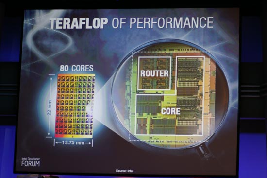
3 / 64 = 4.7%

他没说几个


1T

鬼知道是不是和xbox3一样全部加一起算
那个时候可能1t根本不算什么

也许只是集成显卡的替代品而已
属于低档货

卖自己的集成主板而已
作者: ximimi    时间: 2006-9-28 13:46
说不定就是集成显卡sharder化的未来版

利用一下自己cpu的设计实力而已
作者: RacingPHT    时间: 2006-9-28 13:53
提示: 作者被禁止或删除 内容自动屏蔽
作者: Edison    时间: 2006-9-28 13:58
目前这个东西根据介绍还只是FP簇,能不能跑视频编码还是个很大的问题,毕竟视频编码不仅仅是DCT。
作者: RacingPHT    时间: 2006-9-28 14:02
提示: 作者被禁止或删除 内容自动屏蔽
作者: ximimi    时间: 2006-9-28 14:11
原帖由 RacingPHT 于 2006-9-28 13:53 发表


你完全错了.

集成显卡可以做Linpak吗? 可以算PI吗? 可以让视频编码速度提高数十倍吗? 可以任意做CPU擅长的事情吗? 不行。
这个many core, 可是货真价实的CPU core, 想做什么都可以。本质不同了。

Inte ...

cpu发展到头了就只好搞多功能了

他是代替低端显卡

不是代替u

当然可以做这些

那个时候的显卡说不定把sharder都分出来,通用化了

只要是浮点都可以作
完全可编程
作者: RacingPHT    时间: 2006-9-28 14:33
提示: 作者被禁止或删除 内容自动屏蔽
作者: ximimi    时间: 2006-9-28 14:35
原帖由 RacingPHT 于 2006-9-28 14:33 发表


这招其实我觉得蛮厉害.
至于显卡的shader的通用化, 只要你了解GPU的流水线结构, 就大概会同意, 它和性能相近的core相比完全没有竞争力可言.

与PC上应用面越来越窄的高端GPU相比, 我觉得many core的杀伤力 ...

如果你认为sharder会朝cpu方向发展当然会认为和core比没优势

但是如果他作为另外一种通用的fpga,和cpu争夺同等地位,未必就不是对手了

cpu有累赘
作者: potomac    时间: 2006-10-2 09:34
提示: 作者被禁止或删除 内容自动屏蔽
作者: Edison    时间: 2006-10-2 09:42
原帖由 potomac 于 2006-10-2 09:34 发表

这个bus没看懂。有没有这次IDF的完整PDF下载?:unsure:


ftp://download.intel.com/researc ... /terascale_demo.htm
作者: potomac    时间: 2006-10-2 09:52
提示: 作者被禁止或删除 内容自动屏蔽
作者: RacingPHT    时间: 2006-10-3 12:11
提示: 作者被禁止或删除 内容自动屏蔽
作者: Edison    时间: 2006-10-5 16:37
其实只要有合适容量的cache,目前的CPU都可以以0.25 byte/cycle per flop(stream/linpack)的带宽支撑起来。

http://www.pcinlife.com/article/ ... 59207275d221_8.html
作者: RacingPHT    时间: 2006-10-5 17:36
提示: 作者被禁止或删除 内容自动屏蔽
作者: R620    时间: 2007-2-11 11:16
原帖由 RacingPHT 于 2006-10-3 12:11 发表
单纯图形性能, 这个东西肯定不如专用电路的, 虽然以后flops可能差距不会太大, 但是很多东西, 比如硬件filter, interpolator, MSAA unit, 隐藏延迟的TMU hardware thread, CPU都不好实现。GPU的高端需求, 肯定是 ...


关键是GPU的高端需求所获得的利润能否支持GPU厂商的可持续发展所必须的资金呢?:funk:


欢迎光临 POPPUR爱换 (https://we.poppur.com/) Powered by Discuz! X3.4