POPPUR爱换

标题: 谁有nVIDIA的完整的编年史? [打印本页]

作者: gkke1983    时间: 2007-1-31 22:07
提示: 作者被禁止或删除 内容自动屏蔽
作者: 来不及思考    时间: 2007-1-31 22:09
提示: 作者被禁止或删除 内容自动屏蔽
作者: Trowa    时间: 2007-1-31 22:11
我也想要这么一份资料………………貌似PCI有份图片形式的…………不过好像信息不是很全…………而且那个不方便添加以及时更新………………
作者: 天使之鹰    时间: 2007-2-1 08:41
1.NV3是NVIDIA的第一代具备管线概念的显示芯片,基于它的显卡产品被命名为RIVA 128,但这一代产品并没有GPU的概念,其数据是通过CPU来处理的。不过,顶点和像素管线数目都只有一条,3D性能一般,并且问题较多,算不上一款成功的产品(NV3没有火起来,让NVIDIA在这一时期经济上捉襟见肘,举步维艰)。


基于NV3核心的RIVA 128ZX显卡

另外,基于NV3的显卡还有一款,名为RIVA 128 ZX,管线数和其他参数几乎一样,唯一的区别就是RIVA 128 ZX具备8MB显存,而RIVA 128则只有4MB显存。
作者: 天使之鹰    时间: 2007-2-1 08:44
2.NV4和NV5核心是同一年推出,它们的顶点/像素管线完全相同,均为1个顶点管线和2个像素管线。不同的是,由于生产工艺的改进(NV4的生产工艺为.35um,而NV5则是.25um),它们所集成的晶体管数有很大差距,NV4只有700万晶体管,而NV5却有1500万,是NV3的2倍有余。

基于NV4核心的TNT显卡

应该说TNT是NVIDIA崛起的功臣了,当年由于具备与VOODOO 1相媲美的性能,但价格却比VOODOO 1要便宜近半的价格,在家用3D游戏应用市场迅速打出了一片天地。不过,TNT仍然存在较多问题,所以NVIDIA在不到半年的时间里就推出了它的继任者TNT2。


基于NV5核心的TNT2 Ultra显卡
真正让NVIDIA击败VOODOO显卡的自然是TNT2了。在TNT广受好评的基础上,改进了引擎执行效率、管线传输速度的TNT2发布了,NVIDIA再次成了人们谈论的焦点,因为TNT2的性能表现已经能够超越当时人人羡慕的VOODOOO2显卡了,而且价格更低廉。强劲的性能,低廉的价格,这两个征服市场的必要条件TNT2都具备了,其击败VOODOO自然是在情理之中的事情了。不过,此时的3DFX并未被NVIDIA逼上绝路,他们还有一定机会和实力,然而后面发生的事则彻底让3DFX跌入万劫不复的深渊。
作者: ikinari    时间: 2007-2-1 08:45
提示: 作者被禁止或删除 内容自动屏蔽
作者: 天使之鹰    时间: 2007-2-1 08:47
3.  在TNT2取得了空前胜利之后,NVIDIA并没有停止其前进的步伐,仍然遵守着他每6个月发布一款新品的承诺——其具有划时代意义的GeForce 256发布了。GeForce 256是首个基于GPU概念的产品,GPU将以往需要CPU处理的一些“活”,“揽”了下来,在显示芯片中“就地解决”,大大降低了CPU的负担。这是NVIDIA对于3D图形处理技术发展的最大贡献。并且NV10也是NVIDIA首款具备4条像素渲染管线的显示核心。从那时起,GPU的概念深入人心,管线的光芒完全被当时火热的GPU所掩盖。


基于NV10核心的GeForce 256显卡

从NVIDIA第一款四管线产品推出至今,NVIDIA先后共推出了9款4管线的显示核心,可谓非常丰富,但不同核心,在结构上也有所不同,就像素渲染管道来看,有的是4x1,有的是2x2。4x1的意思是说,4条渲染管道,具备1个着色引擎,2x2是指2条像素渲染管道具备2个着色引擎,是变相的4管线产品。顶点管线也是因核心的不同而不同。

基于NV11核心的GeForce2 MX显卡

其中采用4x1结构的显示核心最多,包括古老的NV10,第五代核心NV31、NV34、NV36和第六代核心NV44及NV44A。NV10对应的产品是GeForce 256;NV31对应的产品是GeForce FX 5600系列,NV34对应的产品是5200系列,NV36对应的是GeForce 5700系列;NV44及NV44A所对应的产品分别是GeForce 6200和6200A系列。其中,基于NV10的顶点管线只有1个,NV31/34/36的顶点管线为2条,而GeForce 5700系列的顶点管线则为3条。

基于NV17核心的低端经典——GeForce4 MX440

采用2x2结构的显示核心,有NV11/17/18三个核心,分别隶属于GeForce2 MX和GeForce4 MX系列,是NVIDIA定位于低端的产品。NV11所对应的产品是基于GeForce 2 MX系列;而NV17/18所对应的产品都是GeForce4 MX系列,不过基于NV18的产品只有一款,就是GeForce4 MX4000。顶点管线方面,NV11/17/18都只具备1条。
作者: 天使之鹰    时间: 2007-2-1 08:50
4.  NVIDIA的任何一代核心,具备8管线的都属于高端产品。自GeForce2开始出现4x2结构的8管线产品起,它就一直保持着高端的姿态,例如,GeForce2 Ti,GeForce3 Ti和GeForce4 Ti以及现在的GeForce 6600显卡等等。

NV最早的8管线产品——GeForce2 Ti显卡(基于NV15核心)

NVIDIA8管线的产品也比较丰富,与4管线一样分为两种结构,一种是4x2,一种是8x1。4x2结构的产品比较老,包括NV15/20/25/28/30/35/38。NV15所对应的产品是GeForce2 GTS/Ti/Pro/Ultra4款当时的高端产品,它们之间的差别只是核心频率和显存频率的不同,管线数是一样的。

基于NV25核心的经典——GeFoce4 Ti4200显卡

   NV20对应的产品是GeForce3 Ti系列产品;NV25/28对应的产品都是GeForce4 Ti系列,其中NV28是为当时的顶级显卡GeForce4 Ti4800单独设计的核心,不过与NV25相比,在特性上没有区别,区别在于NV28能够上到更高的频率。

基于NV30的大家伙——GeForce FX5800显卡(气势不比6800差)

NV30对应的产品是当时为了和ATI Radeon 9700Pro抗衡的GeForce FX 5800系列显卡;NV38对应的产品则是为了与Radeon 9800Pro抗衡的GeForce 5900系列显卡。

基于NVIDIA首款8x1结构的8管线核心——NV43的GeForce 6600GT显卡

其中,NV15/20只具备1个顶点管线,NV25/28则具备2个顶点管线,NV35/38则具备3个顶点管线,基本上每升级一代产品,顶点管线都增加一个。

    8x1结构的核心,在NVIDIA第六代产品中才被采用,并且只有NV43一款核心。他所对应的产品是大家最为熟悉的了——GeForce 6600系列产品。从这款核心衍生的产品非常之多,既有PCI-E平台的也有AGP平台的,包括6600标准版,6600GE,6600GT三大系列。
作者: 天使之鹰    时间: 2007-2-1 08:51
5. 在被ATI的9XXX系列显卡弄得灰头土脸之后,NVIDIA在2004年发布了第六代显GeForce 6800显卡,无论从从性能还是特性上来说,GeForce6800都要略好过ATI的X800,可以说在去年NVIDIA打了一个漂亮的翻身仗。紧接着NVIDIA又发布了GeForce 6800的升级版本6800GT和6800Ultra。

基于NV40核心的昔日“擎天柱”——GeForce 6800Ultra显卡

GeForce 6800GT/Ultra在特性上与GeForce 6800一样,只是像素渲染管线比GeForce 6800多出了一倍,达到了16条,性能提升也几近一倍。GeForce 6800GT和GeForce 6800Ultra的核心是重新设计的,代号为NV40U。而且,6800GT/Ultra的顶点管线也达到了6条。
作者: 天使之鹰    时间: 2007-2-1 08:57
原帖由 ikinari 于 2007-2-1 08:45 发表
传说中未被Dream Cast使用的NV2有资料否~~

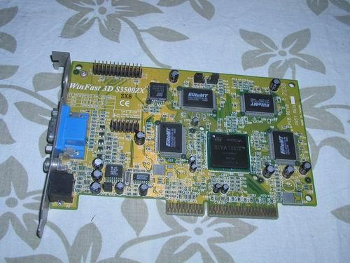
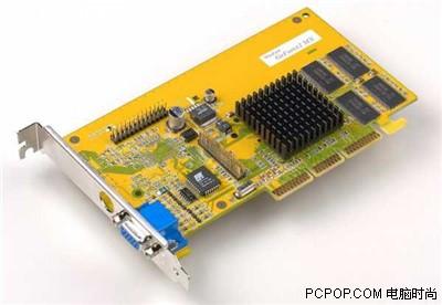
NV1DIAMOND 帝盟 EDGE 3D 3400XL 芯片组:nVidia NV1 nVidia 的第一块显示芯片     台湾著名的 DearHoney 数位音乐工作室 是这么评价此卡的:“這一張是史上第一張 ...

黄仁勋在LSI Logi平步青云,但到1992年底,一个更有挑战性的机会摆到面前。

   黄仁勋在为LSI Logi工作的过程中,结识了克里斯(Chris Malachowsky)与普雷艾姆(Curtis Priem),两人以前都是太阳微系统(Sun Microsystems)的工程师,渐渐觉得应该干一件过瘾的事情,成立一家图形芯片公司。

   克里斯与普雷艾姆找到黄仁勋,力邀既懂技术又擅管理且年龄最小的黄仁勋加盟,一起创业,并担任首席执行官。而此时年届而立之年,在LSI Logi干了8年的黄仁勋正摩拳擦掌,准备开创自己的天地,三人一拍即合,黄仁勋担任总裁兼首席执行官,克里斯担任副总裁,普雷艾姆担任首席技术官。

   1993年1月,Nvidia正式成立。据说,黄仁勋还把第一天上班的时间定在2月17日,刚好是他30岁生日。不管是有意,还是巧合,黄仁勋兑现了自己30岁成立自己公司的诺言。

   在1993年进军图形芯片,这是一个非常大胆但算不上极具开创性的主意。据Bay Area公司图形芯片业的分析师乔恩(Jon Peddie)回忆说:“当时黄仁勋还专门打电话,咨询关于图形芯片市场与未来的走势,我告诉他,这个市场上还没起步已经乱成一团了,现在已经有将近30家公司,你最好别干这个。”

   黄仁勋后来对乔恩开玩笑说,那是他没有采纳的最好的建议。

   乔恩的说法并没有夸张。1993年,英特尔刚刚推出80586,并给这个系列取名奔腾。这位芯片巨头当时最大的努力就是甩开AMD,至于图形芯片还无暇顾及;SGI仍然只给一些工作站提供图形加速器;LSI Logi也尚未专做图形芯片;已经成立8年的ATI自己仍没什么产品,还在吃代工(OEM)市场;Matrox尚未专做显卡;Rendition(1993年成立)以及后来掀起3D革命的3Dfx(1994年成立)尚未出生。连微软的DOS系统都还尚未一统天下,更谈不上什么标准。

   更何况,当时显卡与声卡集成在一起,尚未形成专门的独立芯片市场。可以说,图形芯片市场接近于一张白纸,白得连一个箭头都没有。黄仁勋认为,这是领跑的绝好时机。

   黄仁勋费尽周折,拉来风险投资之后,马上组织研发,力图掀起一场革命。1995年,Nvidia终于推出第一款图形芯片产品NV1,但出乎黄仁勋预料,NV1没人叫好。

   黄仁勋通过总结意识到,此时的Nvidia还欠缺很多东西。首先,在摩尔定律主宰的IT界,两年时间才开发一款产品,本身就是一种失败。其次,NV1并不是专门的图形芯片,它集图形处理、声卡及游戏操作杆等功能于一体。还有,Nvidia只是一家无名小卒,没有几家显卡生产商愿意跟它走。

   最重要的,NV1选择了只有几家游戏机公司看好的正方形成像技术,而其它公司有的选择三角形,有的选择多边形,没有标准,也没有龙头。

   参与NV1研发的Nvidia副总裁克里斯回忆说:“我们最大的错误是NV1采取了集成战略,在显卡上集成了声卡、游戏柄等多项功能,而当时的个人电脑市场正力图将三者分开。”

   黄仁勋后来也承认,NV1的多项技术都非常领先,但这个产品是失败的,因为主流变了,产品根本卖不出去。

   当时最大的主流不是来自3Dfx,而是在整个图形芯片业群龙无首,没有标准的时候,微软推出了Windows95,很快风行世界,成为操作系统的霸主,全球几乎所有软件与硬件开发商都转向Windows95。更重要的是,微软这一年趁机收购一家英国的图形标准公司,利用对方的技术,很快开发出属于微软的图形接口Direct3D标准,支持多边形成像技术,很快号令天下。而英特尔仍在致力于大集成战略,没有意识显示芯片独立的契机。

   微软这一招无异于宣布,黄仁勋跑多快都白跑了,因为微软已经确立了新方向。

   而此时,Nvidia第一笔风险投资已经花得所剩无几,黄仁勋只能痛苦地宣布裁员。他试图再拉一笔风险投资,但失败了。就在Nvidia揭不开锅的时候,游戏机巨头世嘉递来了橄榄枝。

   1995年,索尼还没有推出PS,微软更没有进军XBOX,所以日本游戏机巨头主要就是世嘉与任天堂。当时,世嘉刚好推出一款新游戏机,叫土星,准备用它大战市场。巧合的是,Windows95在日本还没有流行,而土星刚好支持正方形成像技术。更巧的是,NV1附加功能中的游戏操作杆就是以世嘉为模本。所以世嘉就找到Nvidia,请它开发土星游戏机的第二代图形芯片,并给了700万美元订金。真是天不绝Nvidia!

   黄仁勋承认,如果当时没有世嘉这700万美元订金,Nvidia肯定早就消失了,但即便有了这700万美元,Nvidia同样差一点消失,因为Nvidia仍然对自己的技术方向执迷不悟,气得世嘉差点解除合同。

   更重要的,历经一年多时间研发出来的NV2几乎就是个废品,因为市场上已经有明确的标准,而这款产品与主流格格不入。
作者: ikinari    时间: 2007-2-1 09:01
提示: 作者被禁止或删除 内容自动屏蔽
作者: Eureka    时间: 2007-2-1 09:03
原帖由 来不及思考 于 2007-1-31 22:09 发表
这个,以后我收集下资料,我来做吧 :)


支持 ~! 斑竹作个电子书格式的 方便翻阅
作者: 天使之鹰    时间: 2007-2-1 09:07
上传一个Excel附件,包含了除G80的所有NV桌面芯片的参数,希望对大家能有所帮助。
作者: 天使之鹰    时间: 2007-2-1 09:09
原帖由 来不及思考 于 2007-1-31 22:09 发表
这个,以后我收集下资料,我来做吧 :)


思考兄,不好意思,我先下手了,呵呵。

零零散散从网上搜集的资料,你再完善一下做个PDF格式的吧。
作者: gkke1983    时间: 2007-2-1 11:19
提示: 作者被禁止或删除 内容自动屏蔽
作者: Edison    时间: 2007-2-1 11:22
NVIDIAFrom Wikipedia, the free encyclopedia(Redirected from Nvidia)
Jump to: navigation, search
[tr]Type[td]Public (NASDAQ: NVDA)[tr]Founded[td]1993[tr]Headquarters[td]Santa Clara, California, USA[tr]Key people[td]Jen-Hsun Huang, CEO[tr]Industry[td]Semiconductors- Specialized[tr]Products[td]Graphics processing units
Motherboardchipsets[tr]Revenue[td]$2.375 Billion USD (2005)[tr]Net income[td]$302.5 Million USD (2005)[tr]Employees[td]over 3,000 (2006)[tr]Slogan[td]The Way It's Meant to Be Played[tr]Website[td]www.nvidia.com
NVIDIA Corporation
NVIDIA Corporation (NASDAQ: NVDA) (pronounced /ɛnˈvɪdɪə/) is a major supplier of graphics processors (graphics processing units, GPUs), graphics cards, and media and communications devices for PCs and game consoles such as the original Xbox and the PlayStation 3. NVIDIA's most popular product lines are the GeForce series for gaming and the Quadro series for Professional Workstation Graphics processing as well as the nForce series of computer motherboard chipsets. Its headquarters is located at (37°22′14.62″N, 121°57′49.46″W) 2701 San Tomas Expressway, Santa Clara, California.
The name "NVIDIA" is designed to sound like the word "video" and the Spanish envidia ("envy"). [citation needed]
In 2000 it acquired the intellectual assets of one-time rival 3dfx, one of the biggest graphics companies of the mid to late 1990s.
On 2005-12-14, NVIDIA acquired ULI Electronics. ULI supplies third party Southbridge parts for ATI chipsets. In March 2006 NVIDIA acquired Hybrid Graphics [1]and on 2007-01-05, it announced that it had completed the acquisition of PortalPlayer, Inc. [2]
Contents
ProductsNVIDIA's product portfolio includes graphics processors, wireless communications processors, PC platform (motherboard core-logic) [chipsets], and digital media player software. Within the Mac/PC user community, NVIDIA is best known for its "GeForce" product line, which is not only a complete line of "discrete" graphics chips found in AIB (add-in-board) video cards, but also a core-technology in both the Microsoft Xbox game-console and nForce motherboards.
In many respects, NVIDIA is similar to its competitor ATI, because both companies began with a focus in the PC market, but later expanded their businesses into chips for non-PC applications. NVIDIA does not sell graphics boards into the retail market, instead focusing on the development and manufacturing of GPU chips. As part of their operations, both ATI and NVIDIA do create "reference designs" (board schematics) and provide manufacturing samples to their board partners such as ASUS.
In December 2004, it was announced that NVIDIA would be assisting Sony with the design of the graphics processor (RSX) in the upcoming Sony PlayStation 3 game-console. As of March 2006, it is known that NVIDIA will deliver RSX to Sony as an IP-core, and that Sony alone would be responsible for manufacturing the RSX. Under the agreement, NVIDIA will provide ongoing support to port the RSX to Sony's fabs of choice (Sony and Toshiba), as well as die-shrinks to 65nm. This is a departure from NVIDIA's business arrangement with Microsoft, in which NVIDIA managed production and delivery of the Xbox GPU through NVIDIA's usual third-party foundry contracts. (Meanwhile, Microsoft has chosen ATI to provide the IP design for the Xbox 360's graphics hardware, as has Nintendo for their Wii console to supersede the ATI-based GameCube.)
Graphics chipsets Personal computer platforms / chipsets Market history Pre-DirectXNVIDIA's original graphics card called the NV1 was released in 1995, based upon quadratic surfaces, with an integrated playback only soundcard and ports for Sega Saturn gamepads. Because the Saturn was also based upon forward-rendered quads, several Saturn games were converted to NV1 on the PC, such as Panzer Dragoon and Virtua Fighter Remix. However, the NV1 struggled in a market place full of several competing proprietary standards.
Market interest in the product ended when Microsoft announced the DirectX specifications, based upon polygons. Subsequently NV1 development continued internally as the NV2 project, funded by several millions of dollars of investment from Sega. Sega hoped an integrated sound and graphics chip would cut the manufacturing cost of their next console. However, even Sega eventually realized quadratic surfaces were a flawed implementation, and there is no evidence the chip was properly debugged. The NV2 incident remains something of a dark corporate secret for NVIDIA.
A fresh startNVIDIA's CEO Jen-Hsun Huang realized at this point after two failed products, something had to change if the company was to survive. He hired David Kirk, Ph.D. as Chief Scientist from software developer Crystal Dynamics, a company renowned for the visual quality of its titles. David Kirk turned NVIDIA around by combining the company's 3D hardware experience, with an intimate understanding of practical implementations of rendering.
As part of the corporate transformation, NVIDIA abandoned proprietary interfaces, sought to fully support DirectX, and dropped multimedia functionality, in order to reduce manufacturing costs. NVIDIA also adopted an internal 6 month product cycle goal. The future failure of any one product would not threaten the survival of the company, since a next generation replacement part would always be available.
However, since the Sega NV2 contract was secret, and employees had been laid off, it appeared to many industry observers that NVIDIA was no longer active in research and development. So when the RIVA 128 was first announced in 1997, the specifications were hard to believe: Performance superior to market leader 3dfx Voodoo Graphics, and a full hardware triangle setup engine. The RIVA 128 shipped in volume, and the combination of its low cost and high performance 2D/3D acceleration made it a popular choice for OEMs.
Market leadershipHaving finally developed and shipped in volume the market leading integrated graphics chipset, NVIDIA set the internal goal of doubling the number of pixel pipelines in its chip, in order to realize a substantial performance gain. The TwiN Texel (RIVA TNT) engine NVIDIA subsequently developed, allowed either for two textures to be applied to a single pixel, or for two pixels to be processed per clock cycle. The former case allowing for improved visual quality, the latter doubling maximum fill rate.
New features included a 24-bit Z-buffer with 8-bit stencil support, anisotropic filtering, and per-pixel MIP mapping. In certain respects such as transistor count, the TNT had begun to rival Intel's Pentium processors for complexity. However, while the TNT offered an astonishing range of quality integrated features, it failed to displace the market leader Voodoo 2, because the actual clock speed ended up at only 90 MHz, about 35% less than expected.
However, this was only a temporary respite for Voodoo, as NVIDIA's refresh part was a die shrink for the TNT architecture from 350 nm to 250 nm. Stock TNTs now ran at 125 MHz, ULTRAs at 150 MHz. The Voodoo 3 was barely any faster and lacked features such as 32-bit color. The RIVA TNT2 marks a major turning point for NVIDIA. They had finally delivered a product competitive with the fastest on the market, with a superior feature set, strong 2D functionality, all integrated onto a single die with strong yields, that ramped to impressive clock speeds.
The GeForce eraThe fall of 1999 saw the release of the GeForce 256 (NV10), most notably bringing on-board transformation and lighting. The GF256 ran at 120 MHz and was also implemented with advanced video acceleration, motion compensation, hardware sub picture alpha-blending, and had four-pixel pipelines. When combined with DDR memory support, NVIDIA's technology was the hands down performance leader.
Basking in the success of its products, NVIDIA won the contract to develop the graphics hardware for Microsoft’s Xbox. The result was a huge $200 million advance. However, the project drew the time of many of NVIDIA's best engineers. In the short term, this was of no importance, and the GeForce 2 GTS shipped in the summer of 2000.
The GTS benefited from the fact NVIDIA had by this time acquired extensive manufacturing experience with their highly integrated cores, and as a result they were able to optimise the core for clock speeds. The volumes of chips NVIDIA was producing also enabled them to bin split parts, picking out the highest quality cores for their premium range. As a result, the GTS shipped at 200 MHz. The pixel fill rate of the GF256 nearly doubled, and texel fill rate nearly quadrupled because multi-texturing was added to each pixel pipeline. New features included S3TC compression, FSAA, and improved MPEG-2 motion compensation.
More significantly, shortly afterwards NVIDIA launched the GeForce 2 MX, intended for the budget / OEM market. It had two pixel pipelines fewer, and ran at 175 and later, 200 MHz. Offering strong performance at a bargain basement price, the GeForce 2MX is probably the most successful graphics chipset of all time. A mobile version called the GeForce2 Go was also shipped at the end of 2000.
All of which finally proved too much for 3dfx whose Voodoo 5 had been delayed, and the board of directors started the process of dissolving 3dfx. This became one of the most spectacular and public bankruptcies in the history of personal computing. NVIDIA purchased 3dfx primarily for the intellectual property which was in dispute at the time, but also acquired anti-aliasing expertise, and about 100 engineers.
Shortcomings of FX seriesAt this point NVIDIA’s market position looked unassailable, and industry observers began to refer to NVIDIA as the Intel of the graphics industry. However while the next generation FX chips were being developed, many of NVIDIA’s best engineers were working on the Xbox contract, developing a motherboard solution, including the NVIDIA APU used as part of the SoundStorm platform.
It is also worth noting Microsoft paid NVIDIA for the chips themselves, and the contract did not allow for falling manufacturing costs, as process technology improved. Microsoft eventually realized its mistake, but NVIDIA refused to renegotiate the terms of the contract. As a result, NVIDIA and Microsoft relations, which had previously been very good, deteriorated. NVIDIA was not consulted when the DirectX 9 specification was drawn up.[citation needed] Apparently as a result, ATI designed the Radeon 9700 to fit the DirectX specifications. Rendering color support was limited to 24 bits floating point, and shader performance had been emphasized throughout development, since this was to be the main focus of DirectX 9. The Shader compiler was also built using the Radeon 9700 as the base card.
In contrast, NVIDIA’s cards offered 16 and 32 bit floating point modes, offering either lower visual quality (as compared to the competition), or slow performance. The 32 bit support made them much more expensive to manufacture requiring a higher transistor count. Shader performance was often only half or less the speed provided by ATI's competing products.[citation needed] Having made its reputation by providing easy to manufacture DirectX compatible parts, NVIDIA had misjudged Microsoft’s next standard, and was to pay a heavy price for this error. As more and more games started to rely on DirectX 9 features, the poor shader performance of the GeForce FX series became ever more obvious. With the exception of the FX 5700 series (a late revision), the FX series lacked performance compared to equivalent ATI parts.
NVIDIA started to become ever more desperate to hide the shortcomings of the GeForce FX range. A notable 'FX only' demo called Dawn was released, but the wrapper was hacked to enable it to run on a 9700, where it ran faster despite a perceived translation overhead. NVIDIA also began to include ‘optimizations’ in their drivers to increase performance. While some that increased real world gaming performance were valid, hardware review sites started to run articles showing how NVIDIA’s driver autodetected benchmarks, and produced artificially inflated scores that did not relate to real world performance. Often it was tips from ATI’s driver development team that lay behind these articles. As NVIDIA’s drivers became ever more full of hacks and ‘optimizations,' the legendary stability and compatibility also began to suffer. While NVIDIA did partially close the gap with new instruction reordering capabilities introduced in later drivers, shader performance remained weak, and over-sensitive to hardware specific code compilation. NVIDIA worked with Microsoft to release an updated DirectX compiler, that generated GeForce FX specific optimized code.
Furthermore, the GeForce FX series also ran hot, because they drew as much as double the amount of power as equivalent parts from ATI. The GeForce FX 5800 Ultra became notorious for the fan noise, and acquired the nicknames ‘dustbuster’ and 'leafblower'.[citation needed] While it was withdrawn and replaced with quieter parts, NVIDIA was forced to ship large and expensive fans on its FX parts, placing NVIDIA's partners at a manufacturing cost disadvantage compared to ATI. As a result of the FX series' weaknesses, NVIDIA quite unexpectedly lost its market leadership position to ATI.
Dominance in discrete desktop cardsAccording to a survey[3] conducted by Jon Peddie Research, a leading market watch firm, concerning the state of the graphics market in Q2 2006 show that, while NVIDIA's market share in graphics chips overall remained at 3rd place at 20.30%, it is the dominant force in the discrete graphic card solution with a market share of about 51.5%.
Lack of Free software supportMain article: NVIDIA and FOSS
NVIDIA does not provide the documentation for their hardware, which is necessary in order for programmers to write appropriate and effective open source drivers for NVIDIA's products. Instead, NVIDIA provides their own binary GeForce graphics drivers for X.Org and a thin open-source library that interfaces with the Linux, FreeBSD or Solaris kernels and the proprietary graphics software. NVIDIA's Linux support has promoted mutual adoption in the entertainment, scientific visualization, defense and simulation/training industries, which have been traditionally dominated by SGI, Evans & Sutherland and other relatively costly vendors.
Because of the proprietary nature of NVIDIA's drivers, they are at the center of an ongoing controversy within the Linux and FreeBSD communities. Many Linux and FreeBSD users insist on using only open-source drivers, and regard a binary-only driver as wholly inadequate.[citation needed] However, there are also users that are content with the NVIDIA-supported drivers.
Original Equipment ManufacturersNVIDIA doesn't manufacture video cards, just the GPU chips. The cards are assembled by OEMs, and will have one of these brand names:
See also References
External links

NVIDIA Gaming Graphics Processors
Early Chips: NV1NV2
DirectX 5/6: RIVA 128RIVA TNTRIVA TNT2
DirectX 7.x: GeForce 256GeForce 2
DirectX 8.x: GeForce 3GeForce 4
DirectX 9.x: GeForce FXGeForce 6GeForce 7
Direct3D 10: GeForce 8
Other NVIDIA TechnologiesnForce: 220/415/4202SoundStorm34500600Professional Graphics: QuadroQuadro PlexGraphics Card Related: TurboCacheSLISoftware: GelatoCgPureVideoConsumer Electronics: GoForceGame Consoles: Xbox (NV2A)PlayStation 3 (RSX)
作者: gkke1983    时间: 2007-2-1 11:23
提示: 作者被禁止或删除 内容自动屏蔽
作者: Edison    时间: 2007-2-1 11:26
ATI TechnologiesFrom Wikipedia, the free encyclopedia
Jump to: navigation, search
[tr]Type[td]Subsidiary of AMD[tr]Founded[td]1985[tr]Headquarters[td]Markham, Ontario, Canada[tr]Key people[td]David E. Orton, CEO[tr]Industry[td]Semiconductors[tr]Products[td]Graphics cards
Graphics processing units
Motherboard chipsets
Video capture cards[tr]Revenue[td]$2.222 Billion USD (2005)[tr]Net income[td]$16.93 Million USD (2005)[tr]Employees[td]3,469 (2005)[tr]Owner[td]AMD[tr]Slogan[td]Get In the Game[tr]Website[td]ati.amd.com
ATI Technologies U.L.C.

ATI Technologies U.L.C., founded in 1985, is a major designer of graphics processing units and video display cards and a wholly owned subsidiary of AMD, as of October 2006.

As a fabless semiconductor company, ATI conducts research & development of chips in-house, but subcontracts the actual (silicon) manufacturing and graphics-card assembly to third-parties.

On July 24, 2006, AMD and ATI announced a plan to merge together in a deal valued at US$5.4 billion. The merger closed October 25, 2006 (Press Release). The acquisition consideration included over $2 billion financed from a loan, as well as 56 million shares of AMD stock. [1]

Contents
History
ATI's Silicon Valley office.


ATI was founded under the name Array Technologies Incorporated in 1985 by three Chinese immigrants, China-born Kwok Yuen Ho [2] and Hong Kong-born Benny Lau and Lee Lau. Array Technologies primarily worked in the OEM field, producing integrated graphics chips for large PC manufacturers like IBM. By 1987 it had evolved into an independent graphics card retailer, marketing the EGA Wonder and VGA Wonder graphics cards under its own ATI moniker.

In 1997 ATI acquired Tseng Labs's graphics assets, which included 40 new engineers. In 2000, ATI acquired ArtX, the company that engineered the "Flipper" graphics chip used in the Nintendo GameCube games console. They have also entered an agreement with Nintendo to create the chip for the successor of the GameCube, named Wii. ATI was contracted by Microsoft to create the graphics chip for Microsoft Xbox 360. Later in 2005, ATI acquired Terayon's Cable Modem Silicon Intellectual Property cementing their lead in the consumer digital television market (press release).

Its current President and CEO is David E. Orton (formerly of ArtX). K. Y. Ho remained as Chairman of the Board until he retired on November 22, 2005.

ATI was acquired by AMD for $5.4 billion on October 25, 2006. [3]. The merger was approved by Markham, Ontario, Canada-based ATI shareholders and U.S. & Canadian regulators. Even though now owned by AMD, ATI will retain its name, logos, and trademarks. It will continue to function as a separate division focused solely on the production & development of graphics technologies.[4]
[url=][/url]
ProductsIn addition to developing high-end GPUs (graphics processing unit, something ATI calls a VPU, visual processing unit) for PCs, ATI also designs embedded versions for laptops (called "Mobility Radeon"), PDAs and mobile phones ("Imageon"), integrated motherboards ("Radeon IGP"), set-top boxes ("Xilleon") and other technology-based market segments. Thanks to this diverse portfolio, ATI has been traditionally the dominant player in the OEM and multimedia markets.

Currently ATI is the main competitor of NVIDIA. As of 2004, ATI's flagship product line is the Radeon series of graphics cards which directly compete with those boards using NVIDIA's GeForce GPUs. As of the 3rd quarter of 2004, ATI represented 59% of the discrete graphic card market, while its primary competitor NVIDIA represented only 37%, but the two commonly trade market share majority, for example 2nd quarter had NVIDIA at 50% and ATI at 46%.

As of 2005, ATI has announced that a deal has been struck with CPU and Motherboard manufacturers, particularly Asus and Intel, to create onboard 3D Graphics solutions for Intel's new range of motherboards that will be released with their new range of Intel Pentium M-based desktop processors, the Intel Core and Intel Core 2 processors. This ATI solution will effectively end Intel's range of entry-level desktop integrated graphics. However, high-end boards with integrated graphics will still use Intel integrated graphics processors.
Computer graphics chipsetsThis list is incomplete; you can help by expanding it.

A Radeon X1900 series graphics card.


Console graphics solutions Handheld chipsets Personal computer platforms & chipsetsEarly north bridge parts produced by ATI included the Radeon 320, 340 and 7000. Typically these were partnered with a south bridge chip from ULI. They sold in respectable volumes, but never gained enthusiast support.

In 2003 ATI released the 9100 IGP[5], with IXP250 southbridge. It was notable for being ATI's first complete motherboard chipset, including an ATI southbridge, admittedly light on features, but stable and functional. It included an updated Direct-X 8.1 class version of the 8500 core for the integrated graphics, based upon the 9100. Internally, ATI considered it one of their most important product launches.

The Xpress 200/200P is ATI's PCI Express-based Athlon 64 and Pentium 4 motherboard chipset. The chipset supports SATA as well as integrated graphics with DirectX 9.0 support, the first integrated graphics chipset to do so. The graphics is based on an X300 core integrated into the north bridge, with two pixel pipelines operating at a core speed of up to 350 MHz, each one having a single texturing unit.

In 2006, ATI Released the Xpress 3200, a true Crossfire solution. Where the XPRESS 200 (2x PCIe x8 or 1xPCIe x16) is not designed specifically for Crossfire, the Xpress 3200 (2x PCIe x16) is. Because both x16 slots are connected to one physical chip, ATI has been able to accelerate the link between both graphics card slots in order to compensate for the lack of a dedicated GPU-to-GPU interconnect.
Operating system driversATI currently provides proprietary drivers for Microsoft Windows XP, Mac OS X, and Linux. Linux users have the option of both the old proprietary (R200 and above) and new open source (R480 and below) drivers. More details can be found on the Radeon page. In an interview with AMDs Hal Speed it was suggested that AMD were strongly considering open sourcing at least a functional part of the ATI drivers. [6]. However, at least until the merger with AMD was complete, ATI had no plans to open source their drivers:

Proprietary, patented optimizations are part of the value we provide to our customers and we have no plans to release these drivers to open source. In addition, multimedia elements such as content protection must not, by their very nature, be allowed to go open source.
—the company said in a statement, [7]


In April 2006, when an ATI representative was to speak at the MIT campus in the same building where the Free Software Foundation rents their offices, Richard Stallman organised a protest against ATI on the grounds that ATI does not release the documentation of their hardware, thus making it largely impossible to write free software drivers for their graphics adapters. For the duration of ATI's speech, Stallman was holding a sign that said "Don't buy from ATI, enemy of your freedom". Although Richard Stallman had no intention of disrupting the speech, and indicated that the sign was loud only visually, the organisers of the speech brought a police officer to the scene, although they had failed to provide the officer with a valid reason for his presence at the event, according to the FSF web-site. [8]
[url=][/url]
Market trendsATI was founded in 1985, and in order to survive, initially ended up shipping a lot of basic 2D graphics chips to companies such as Commodore. The EGA Wonder and VGA Wonder families were released to the PC market in 1987. Each offered enhanced feature sets surpassing IBM's own (EGA and VGA) display adapters. May of 1991 saw the release of the Mach8 product, ATI's first "Windows accelerator" product. Windows accelerators offloaded display-processing tasks which had been performed by the CPU. (In fact, the Mach8 was feature-enhanced IBM 8514/A-compatible board.) 1992 saw the release of the Mach32 chipset, an evolutionary improvement over its predecessor.
Modern integrated chipsetsBut it was probably the Mach64 in 1994, powering the Graphics Xpression and Graphics Pro Turbo, that was ATI's first recognizably modern media chipset. Notably, the Mach64 chipset offered hardware support for YUV-to-RGB color space conversion, in addition to hardware zoom. This effectively meant basic AVI and MPEG-1 playback became possible on PCs without the need for expensive specialized decoding hardware. Later, the Mach64-VT allowed for scaling to be offloaded from the CPU. ImpacTV in 1996 went further with 800x600 VGA-to-TV encoding. ATI priced the product at a point where the user effectively got a 3D accelerator for free.

ATI’s first integrated TV tuner products shipped in 1996, recognizable as the modern All-in-Wonder specification. These featured 3D acceleration powered by ATI's second generation 3D Rage II, 64-bit 2D performance, TV-quality video acceleration, video capture, TV tuner functionality, flicker-free TV-out and stereo TV audio.

However, while ATI had established a reputation for quality multimedia-capable cards popular with OEMs, by the late 1990s consumers began to also expect strong 3D performance, and 3dfx and NVIDIA were delivering. The first warning was seen with in January 1999 with the All-in-Wonder 128, featuring the Rage 128 GL graphics chip. While the basic 16 MiB version sold reasonably well, the improved but delayed 32 MiB version did not, because it lacked 3D acceleration appropriate for its price point. It became clear that if ATI was to survive, the company would have to develop integrated 3D acceleration competitive with the products NVIDIA was designing.
Improved 3D performanceATI’s first real 3D chip was the 3D Rage II. The chip supported bilinear and trilinear filtering, z-buffer, and several Direct3D texture blend modes. But the pixel fillrate looked good only next to S3’s VIRGE cards, which were of very poor quality for the time, and the feature list looked good only next to the workstation type Matrox Mystique.

The 3D Rage Pro, released in 1997, offered an improved fill rate equal to the original 3dfx Voodoo Graphics, and a proper 1.2 M triangle/s hardware setup engine. Single-pass trilinear filtering combined with a complete texture blending implementation. The Rage Pro sold in volume to OEMs due to its DVD performance and low cost, but was held back by poor drivers. It was only in 1999, almost two years after the original launch, the drivers finally achieved their potential, delivering a 20-40% gain over the originals. Subsequently ATI learned to better prioritise driver development.

Work on the next-generation 128 GL was helped by the acquisition of the Tseng development team in 1997. Designed to compete with the RIVA TNT and Voodoo2, it was notable for its advanced memory architecture which allowed the Rage128 to run in 32-bit color modes with minimal performance losses. Unfortunately, at the time most games ran in 16-bit color modes, where NVIDIA's parts excelled.

The RIVA TNT2 came out with improved clock speeds, and the GL quickly became relegated to ATI's usual position: that of a strong OEM alternative to the market leaders, with outstanding DVD performance, attractive when priced low enough.
The part was updated in April 1999 with the Rage 128 Pro, featuring anisotropic filtering, a better triangle setup engine, and a higher clock rate. The Rage 128 Pro's MPEG-2 acceleration was far ahead of its time, allowing realtime MP@HL (1920x1080) playback on a Pentium III 600 MHz. ATI also ran an experimental project called "Project Aurora," marketed as the MAXX technology, consisting of dual Rage 128 Pro chips running in parallel, with each chip rendering alternate frames. Because the MAXX required double the memory, suffered from buggy drivers, and failed to deliver knockout performance, it was not a successful launch. As a result, ATI discontinued multiple chip development for mainstream products.
Radeon lineBy this point the pattern seemed clear: ATI was good at producing low-end OEM-friendly parts with good 2D features, DVD acceleration, and rounded 3D feature sets. What they had failed to do was challenge effectively at the high end of the market. So, at the Game Developer's Conference in March 2000, developers were curious but generally somewhat skeptical about a new claimed sixth-generation graphics chip. This was a period when companies often announced products that they failed to deliver on time, or on spec. However, ATI subsequently demonstrated beta silicon behind closed doors at GDC, and named the product the Radeon 256.

The original Radeon core (R100) was released in 2000. ATI's new video card based on this core was originally named the Radeon 64 VIVO to emphasize its 64 MiB of DDR memory and video features, but was eventually renamed the Radeon 7200, reflecting its DirectX 7-compliant feature set. The R100 core established a number of notable firsts, such as a complete DX7 bump-mapping implementation (emboss, dot product 3, and EMBM), hardware 3D shadows, hardware per-pixel video-deinterlacing, and a reasonable implementation of many advanced DX8 pixel shader effects. Unfortunately, ATI used a 2 pixel pipeline design for the R100 with three raster units per pixel pipeline. NVIDIA's competing GeForce 2 chips had a four pipe design with two raster units per pipeline. Very few 3D applications at the time utilized more than two textures per pixel, and thus the third raster units in the Radeon were seldom utilized.

ATI proved the original Radeon had not been a one-off by following up with the second generation Radeon (R200) core in 2001, marketed as the Radeon 8500. The R200 raster pipeline arrangement matched the design of the NVIDIA's GeForce 2 series with four pipelines with two raster units per pipeline. ATI was shooting for 300 MHz core speed for the new 8500, but was unable to reach it. In fact, ATI retail boxes and literature describe the texture fillrate of the 8500 at the 300 MHz speed (2.4 GTexel/s), but the cards were only shipped at 275 MHz speed. NVIDIA quickly released GeForce cards with faster clock speeds. NVIDIA's top GeForce 4 Ti cards delivered greater raw power in terms of fill rates, but ATI started to open up a clear quality and shader performance advantage. In fact, many new games in 2005 still supported the DirectX pixel shader 1.4 of the R200, but not the less capable pixel shader 1.3 units of NVIDIA's latter released GeForce 4 chips
Challenging NVIDIADuring this period ATI also began to sell their core chip technology to third-party "Powered by ATI" board manufacturers, directly competing with NVIDIA’s business model. This change suddenly put NVIDIA on the back foot for the first time since the ill-fated NV1 project, to the amazement of the entire industry. Alongside the Radeon 8500, ATI released a die shrink version (RV200) of the original R100 core which was released as the Radeon 7500. This chip had an extremely fast core clockspeed for the time of 290 MHz with all the features of the original Radeon. ATI also sold a single pipeline version of the original Radeon as the Radeon 7000. Left over R100 chips were sold to third-party video card manufacturers and marketed as the Radeon 7200.

The Radeon 8500 proved popular with OEMs, partly because it offered wider motherboard compatibility than NVIDIA's offerings of the period. The 8500 finally established ATI as a serious performance and feature integrated chipset competitor to NVIDIA, in a period when other graphics card companies such as 3dfx were going out of business. However poorly-written drivers continued to be a notorious weakness of ATI products. ATI responded by introducing their unified "Catalyst" driver/application suite, which attempted to address the quality, compatibility, and performance concerns raised by the user community.
Performance leadershipThe Radeon SE/VIVO and Radeon 8500 cards were warning shots for NVIDIA, demonstrating they could not take for granted their dominant market position. 2002 proved to be the decisive year for ATI, with an unexpected introduction of a new Radeon architecture. The third generation Radeon 9700, based on the R300 core, was designed from the ground up for DirectX 9 operation. Upon its release, it was easily the fastest consumer gaming video card available.[1] Furthermore, ATI beat NVIDIA’s DirectX 9 chip to market by several months and soundly defeated it in almost every application. NVIDIA's "NV30" architecture, while innovative and forward-looking, suffered when advanced features were used, such as pixel/vertex shading, anti-aliasing, and anisotropic filtering. [2]
[url=][/url]
Mainstream valueFrom then onwards, the challenge for ATI became holding onto their high-end advantage, while filtering their technology down to the mid and low end of the market, where the greatest volume sales are made. ATI decided to sell R300 cores with a reduced core clock speed, and half the pixel pipelines disabled, as a midrange product called the Radeon 9500. ATI's own Radeon 9500 Pro card was a R300 core with a 128 bit memory bus running at 275 MHz. This card proved to be just as fast as the fastest GeForce 4 cards and considerably faster than those cards in DirectX 9 applications and most OpenGL applications.

The release of the R300 brought a great deal of interest in ATI from third party manufacturers. To meet the demand for new mid-range cards ATI even allowed manufacturers to sell some Radeon 9700 cards with half their pipelines disabled as Radeon 9500 cards. These differed from the 9500 Pro cards in that they had a 256 bit memory bus, however with only 4 working pipelines their performance was markedly reduced. Soon hardware enthusiasts discovered that it was possible and rather easy to unlock the disabled pipelines on these discounted cards. Eventually, the only thing required to turn these inexpensive Radeon 9500's into full Radeon 9700's was a hacked software driver.

For the low end, ATI released a new value chip (RV250) based on the Radeon R200 core with half the raster units per pipeline. This raster arrangement actually matched the original GeForce design, but the Radeon 9000 also had the same shader processing power and features as the 8500. This DirectX 8.1 capable part competed with NVIDIA's two pipeline, DirectX 7 GeForce 4 MX. Despite having half the fillrate of the Radeon 8500, the Radeon 9000 had very similar performance. ATI also allowed third party manufacturers to continue selling the original R200 cores as Radeon 9100's to reflect the slight performance advantage of the extra raster units. However, the situation was soon confused when the AGP 3.0 refresh of the RV280 was named the Radeon 9200, and when ATI named its new two pipeline integrated chipset the Radeon 9100 IGP.

ATI refreshed the 9700 to the 9800 Pro (R350) in 2003, featuring a small and relatively quiet cooling solution. The 9800 went on to become one of the most popular and best selling enthusiast cards to date. In the midrange market, the 9600 (RV350) was introduced with half the number of pixel pipelines of the 9800 Pro. Adding to the model naming confusion, this card was generally inferior in performance to the Radeon 9500 Pro (R300), but it was cool running. While the pixel fill rate of the Radeon 9600 did not exceed previous generation parts such as the Radeon 8500 (R200) and GeForce 4 series cards, it featured fast and power efficient shader support, offering excellent performance on DirectX 9 and OpenGL based titles. It was refreshed as the 9600XT, gaining another 100 MHz to 500 MHz, from an improved low-k manufacturing process.
Gaining market shareIn 2004, ATI released the RADEON XPRESS 200 motherboard chipset, intended as a direct competitor to the more established nForce motherboard brand of chipsets from arch rival NVIDIA. The 9700 core trickled down into the low end market in the form of a cost-reduced 9600, the 9550, which was fabbed on 0.11u. Even at its core-clock of 250 MHz, the 9550 quickly overtook NVIDIA's 5200 as the favorite entry-level discrete OEM card. As a result, almost unnoticed, ATI completed one of the most surprising turnarounds in recent chip history.

According to data from Mercury Research, ATI Technologies' market share rose by 4 percentage points to 27% in the Q3 2004, while NVIDIA's share dropped 8 points from 23% to 15%. Intel's market share rose 1 point to 39% in the Q3 2004, holding on to the market number one position, although Intel only ships low performance integrated solutions.

In 2005, ATI began shipping the x800 XL PCI-E card, a 110 nm shrink of the x800 core (which originally shipped on a 130 nm low-K process.) This brought 16-pipeline cards closer to the mainstream. The x850 range marks the end of the old 9700 feature set/core as ATI's performance platform. The omission of SM 3.0 and FP32 permitted a more compact die size, allowing ATI to price the X800XL lower than comparable NVidia products.
x1000 seriesThe long-awaited Radeon X1000 series was ATI's first major architectural advancement since the 9700 series. The high end Radeon X1800 had been planned for a mid-2005 release, but the chip did not reach the retail market until October 2005. ATI's first foray into 90nm production was an unhappy one: a silicon-library bug reduced clockable speeds by 150 MHz, delaying R520 production for several months. The missed window of opportunity allowed NVIDIA's 7800 line to dominate the high-end market. As it turned out, the delay of the X1800 led to ATI's entire SM3 product-line launching at roughly the same time: entry-level X1300, mainstream X1600, and high-end/enthusiast X1800. The high end Radeon X1800 managed to maintain parity with the NVIDIA GeForce 7800 GTX. ATI retained slightly greater market share, though margins and profitability slumped.

In January 2006, ATI replaced the short-lived X1800 with the Radeon X1900XT and X1900XTX (R580). With 48 pixel shader units, R580 brought ATI's 3:1 pixel shader to pipeline ratio (first seen on the 12 shader Radeon X1600) to the desktop high end. This enabled ATI to regain the performance crown over the GeForce 7800 GTX 512 in the majority of situations and to an extent, even against the later-released 7900GTX. However, the R580's die-size suggests ATI's performance leadership came at a significant cost. The X1900 (R580) core contains roughly 384 million transistors, in a die size of 352 mm². NVidia's 7900 (G71) core contains roughly 278 million transistors, in a die size of 196 mm². As both devices are known to be manufactured on TSMC's 90nm low-K CMOS logic process, the raw per-die cost of the R580 core is estimated to be twice as much as the NVIDIA part. While the ATI part has a more flexible feature set, the difference in manufacturing cost points to ATI facing near term margin pressure.

On July 21, ATI announced the newest product to the x1000 series, the Radeon X1950XTX(R580+). The X1950XTX will come in two versions, the XTX and Crossfire version, and will feature GDDR4 memory, as opposed to the current GDDR3 memory used in the X1900s. The new core and memory clocks for the X1950s will be 650 MHz and 2 GHz, respectively, compared to the X1900XT with 625/1450 and the XTX with 650/1550. The X1950XTX was presented on August 23, 2006. It is available since mid-September and retails at US$449. On 17 Oct ATI introduced the x1950 PRO based on the new RV570 core, a die shrink to 80nm of the R580, with a reduced 12 pixel pipelines and 36 pixel shaders (the X1900GT had the same configuration, but was a R580 with one pixel quad disabled). A compositing engine is also integrated into the core, so that two X1950 PRO's can now work together, without the need for a mastercard or external dongle. At 230 mm² with 330 million transistors[9], the new die is much cheaper to manufacture.
Stream processingThe R5x series has seen ATI introduce the concept of GPUs as 32-bit (single precision) floating point vector processors. Due to the highly parallel nature of vector processors, this can have a huge impact in specific data processing applications. The mass client project Folding@Home has reported improvements of 20–40 times using an R580 card[10]. It is anticipated in the industry that graphics cards may be used in future game physics calculations.
AVIVOMain article: AVIVO
[url=][/url]
See also
ATI Graphics Processors
2D Chips: Mach
DirectX 3-6: Rage
DirectX 7.x: Radeon R100
DirectX 8.x: Radeon R200
DirectX 9.x: Radeon R300R420
R520
Direct3D 10: Radeon R600
Other ATI TechnologiesChipsets: IGP3xx9000/9100 IGPXpress 200Xpress 3200
580X690GRD700Multi-GPU: Multi-RenderingCrossFireProfessional Graphics: FireGLFireMVConsumer Electronics: ImageonMisc: HyperMemoryAVIVOGame Consoles: GameCube (Flipper) • Xbox 360 (Xenos) • Wii (Hollywood)
作者: hdht    时间: 2007-2-1 12:30
提示: 作者被禁止或删除 内容自动屏蔽
作者: zzhang    时间: 2007-2-1 12:48
嗨,维基百科(wikipedia)上有现成的NVidia和ATi的编年史。我一会儿给你们贴个中文的
作者: zzhang    时间: 2007-2-1 12:59
NVIDIA
维基百科,自由的百科全书
跳转到: 导航, 搜索
NVIDIA Corporation nVidia logo
公司类型         上市公司 (纳斯达克 NVDA)
市场资料         {{{market_information}}}
成立时间         1993
总部地点         美国加利福尼亚州的圣克拉拉
邮政编号         {{{zip_code}}}
电话号码         {{{telephone_no}}}
重要人物         黄仁勋, CEO
口号         The Way It's Meant to Be Played
产业         半导体
产品         显示芯片
主板芯片组
资本金         {{{capital}}}
营业额         盈利$2.375 Billion USD (2005)
税前盈余         {{{operating_income}}}
净利         盈利$302.5 Million USD (2005)
员工数         2,737 (2005)
结算期         {{{accounting_period}}}
母公司         {{{parent}}}
子公司         {{{subsid}}}
网站         www.nvidia.com
{{{footnotes}}}

nVIDIA公司,(NASDAQ: NVDA) (发音: IPA:/ɛnvɪdɪə/) 全称为nVIDIA Corporation,创立于1993年1月,是一家以设计显示芯片和主板芯片组为主的半导体公司。NVIDIA亦会设计游戏 机核心,例如Xbox和PlayStation 3。NVIDIA最出名的产品线是为游戏而设的GeForce显示卡系列,为专业工作站而设的Quadro显示卡系列,和用于电脑主机版的nForce芯片组系列。

NVIDIA的总部设在美国加利福尼亚州的圣克拉拉。是一家无晶圆IC半导体设计公司(Fabless)。"NVIDIA"的读音与英文"video"相似,亦与西班牙文envidia(英文"envy")相似。
目录
[隐藏]

    * 1 历史
    * 2 主要产品
    * 3 显示芯片
    * 4 个人电脑平台 / 芯片组
    * 5 市场历史
          o 5.1 在DirectX前
          o 5.2 一个新颖的开始
          o 5.3 市场领导
          o 5.4 GeForce世代
          o 5.5 GeForce FX的缺点
          o 5.6 效能领导
          o 5.7 独立显卡市场的优势
    * 6 缺乏自由软件的支持
    * 7 原来设备制造商
    * 8 参考
    * 9 外部链接

[编辑] 历史

黄仁勋, Chris Malachowsky和Curtis Priem于1993年1月在美国加州创办了NVIDIA(随后成为德拉威州企业)。NVIDIA保持低调直到1997-1998年,当时它发布了RIVA个人电脑绘图处理器产品线。它于1999年1月在Nasdaq挂牌上市;同年5月,售出第一千万个绘图处理器。于2000年,它收购了一代王者 - 3dfx的知识资产。3dfx是九十年代中期其中一间最大的图形显示厂商。NVIDIA与很多OEM厂商,和一些组织(例如SGI)建立起密切关系。2002年2月,NVIDIA售出第一亿个绘图处理器。

今天,NVIDIA和ATI(已被AMD收购)供应了市场上大部分独立显卡。NVIDIA的旗舰级产品,GeForce绘图处理器产品线,于1999年首次亮相。现在,GeForce产品线已扩充至覆盖桌上型和流动型电脑。便携式装置方面,NVIDIA拥有 Goforce 产品线。它能提供高效能同时,亦能保持低电源消耗。此类产品通常用于无线通讯装置。

作为一家无晶圆IC半导体设计公司,NVIDIA于自己的实验室研发芯片,但将芯片制造工序分包给其他厂商。以往,NVIDIA从其他厂商,例如IBM,意法半导体,台积电和联华电子获得硅生产能力。芯片的供应链需涉及数间第三厂:薄片制造厂,test-house测试核心并根据效能将之分类,和将芯片封装的厂商。依据存货清单,NVIDIA必须提早数月订购芯片,并将之储存起来等待使用。这偶尔会引起供应补给的不稳定。

NVIDIA收购了PACE Soft Silicon,一间位于印度浦那专门生产视讯软件的公司[1],目的是增加NVIDIA在印度的工程师。[2]

于2005年12月14日,NVIDIA收购了宇力电子。宇力电子曾经为ATI的芯片组供应南桥。2006年3月,NVIDIA收购了Hybrid Graphics [3]

NVIDIA亦收购了PORTAL PLAYER Inc.,一间位于美国加州圣荷西的专门生产流动多媒体半导体装置的公司。[4]
作者: zzhang    时间: 2007-2-1 13:01
主要产品

NVIDIA的产品组合包括缯图处理器、无线通讯处理器、个人电脑平台(主版逻辑核心)芯片组和数码媒体播放器的软件。在Mac/PC使用者社群中,NVIDIA的"GeForce"产品线最为人熟悉。除了独立型显卡外,还有Microsoft的Xbox游戏核心和NForce主板的核心技术。

在很多领域,NVIDIA和它的对手ATI很相似。因为两间公司原本只注重PC市场,随后扩展业务至非PC应用芯片。NVIDIA不销售零售版显卡,但专注于研发的制造GPU。ATI和NVIDIA只会提供参考版(俗称公版)给显卡制造商。很多显卡制造商只会根据公版的设计制造显卡,只有少数厂商会特别研发非公版显卡。

在2004年12月,NVIDIA宣布会协助Sony设计PS3的绘图处理器(RSX)。 NVIDIA只会负责设计,Sony会负责制造该绘图处理器。根据合约,NVIDIA会使用新力的芯片厂(新力和东芝)来制造RSX,并将制程提升至65 纳米。这与微软的协议是互相违背的,因为NVIDIA会透过第三者制造Xbox的绘图处理器。(其间微软选择了ATI去提供Xbox 360的绘图硬件的IP设计。任天堂的GameCube和Wii亦采用ATI的绘图处理器。)

    * "Discrete" refers to the graphic chip's boundary/proximity to other PC hardware. A discrete piece of hardware can be physically plugged/unplugged from the motherboard, the opposite term being "integrated graphics" where the piece of hardware is inseparable from the motherboard. In the PC graphics architecture, "discrete" means graphics-hardware is encapsulated in a dedicated (separate) chip. The chip's physical location, whether soldered on the motherboard PCB (as in most laptops) or mounted on an aftermarket add-in-board, has no bearing on this designation.

[编辑] 显示芯片

    * NV1 – NVIDIA的第一款产品,建基于二次曲面。
    * RIVA 128 and RIVA 128ZX – 支援DirectX 5和OpenGL 1, NVIDIA第一款支援DirectX的产品。
    * RIVA TNT, RIVA TNT2 – 支援DirectX 6和OpenGL 1, 这个显卡系列使NVIDIA成为市场领导者。
    * NVIDIA GeForce
          o GeForce 256 – 支援DirectX 7, OpenGL 1, 硬件转换与投影(T&L), 能使用DDR内存作为显示内存。
          o GeForce 2 – 支援DirectX 7和OpenGL 1
          o GeForce 3 – 支援DirectX 8.0著色, OpenGL 1.2, 内存带宽节省技术。
          o GeForce 4 – 支援DirectX 8.1, OpenGL 1.4。低廉的MX系列只支援DirectX 7,因为它是建基于GeForce 2。
          o GeForce FX – 支援DirectX 9和OpenGL 1.5,特色是可以呈现'电影级效果'。
          o GeForce 6 – 支援DirectX 9C, OpenGL 2.0, 特色是一个改进了的著色引擎, 更节省电力的设计和SLI技术。
          o GeForce 7 – 支援DirectX 9C, 'Windows Display Driver Model', OpenGL 2.0。这系列改进了著色效率,率先支援TSAA和TMAA抗锯齿技术,亦支援SLI。
          o GeForce 8 – 支援DirectX 9L和DirectX 10, 采用统一管线结构。它是由顶点、几何和像素著色引擎(统称SM 4.0)组成。支援Luminex引擎,CSAA抗锯齿技术和Quantum Effects。
    * NVIDIA Quadro – 高质素工作站用的专业绘图芯片
    * NVIDIA GoForce – 移动设备用的媒体处理器,多用于PDA, 智能手机和手提电话。备有nPower技术节省电力消耗。
          o GoForce 2150 – 支援一百三十万像素数码镜头, JPEG和2D加速。
          o GoForce 3000 – GoForce 4000的低价版本,功能较少。
          o GoForce 4000 – 支援三百万像素数码镜头,硬件MPEG-4/H.263解码。
          o GoForce 4500 – 曾经用于Gizmondo, 支援3D缯图,拥有几何处理器和可编程像素著色引擎。
          o GoForce 4800 – 支援三百万像素数码镜头和3D缯图。
          o GoForce 5500 – 支援一千万像素数码镜头,第二代3D缯图引擎,24-bit音效引擎和H.264解码。

[编辑] 个人电脑平台 / 芯片组

    * NVIDIA nForce - 原来只可支持AMD平台,在获得Intel的授权后,从nForce4开始连Intel平台亦可支持。
          o nForce IGP (AMD Athlon/Duron K7产品线)
          o nForce2 (AMD Athlon/Duron K7产品线, 北桥被称为SPP (system platform processor) 或 IGP (Integrated Graphics Platform),后者整合了显示芯片。而南桥被称为MCP (Media and Communications Processor), 支援SoundStorm音效)
          o nForce3 (AMD Athlon 64/Athlon 64 FX/AMD Opteron, 南北桥整合的单芯片芯片组,被称为MCP)
          o nForce4 (4X, Base, Ultra和SLi) (支援PCI Express,AMD Athlon 64处理器。SLI版本支援SLI技术)
          o nForce 500 (AMD Athlon 64 FX/Athlon 64 X2/Athlon 64/Sempron 或 Intel Core 2 Extreme/Core 2 Duo/Pentium D/Pentium 4/Celeron D)
          o nForce 600
          o nForce Go 430 - 流动整合形芯片组,集成GeForce Go 6100显视核心。
    * Xbox GeForce3级数显示芯片 (使用Intel Pentium III/Celeron作为平台)
    * PlayStation 3 (RSX 'Reality Synthesizer')

[编辑]
作者: zzhang    时间: 2007-2-1 13:04
市场历史

[编辑] 在DirectX前

NVIDIA的第一张3D显卡是NV1,于1995年推出。它是建基于二次曲面贴图作为立体图形的实现方式。这张卡亦整合了声卡(只能作播放用,并没有音效输入),和世嘉土星游戏手柄和操纵杆的接口。由于世嘉土星是建基于forward-rendered quads,几款世嘉土星的游戏亦被移植到电脑平台。例如铁甲飞龙和VR战士。但是,NV1只能艰难地行进,因为该市场已有很多对手。

之后,市场对NV1失去兴趣,因为Microsoft发布了DirectX规格。它以多边形作为立体图形的实现方式。随后,NV1继续秘密地发展,成为NV2计划。该计划由世嘉资助了几百万元。世嘉希望一个整合了音效和绘图的核心能减低下一代游戏核心的制造成本。但是,世嘉最终了解到二次曲面贴图是有缺点的,最终亦没有证据证明该核心被恰当地除错。这事件成为NVIDIA黑暗的一面。

[编辑] 一个新颖的开始

NVIDIA发布了两款失败的产品后,CEO黄仁勋领悟到公司要继续生存,就必须作出改变。他雇用了David Kirk, Ph.D.作为首席科学家。David Kirk原本是属于软件开发商Crystal Dynamics,一间提供优良视觉品质的公司。他基于对著色的熟悉,将NVIDIA的3D硬件经验合并起来,使NVIDIA得以翻身。

作为企业转形的一部分,NVIDIA放弃了一些专利界面,转为全面支援DirectX,亦弃掉一些多媒体功能,减低制造成本。NVIDIA亦采用了一个为期六个月的内部周期目标。将来,就算某一产品失败,亦不会威胁到公司的生存,因为下一代的代替物随时可用。

但是,自从世嘉NV2的合同隐蔽起来后,雇员都被投闲置散,很多工业观察者都认为NVIDIA不会再活跃于研发工作。所以当RIVA 128在1997年首次推出时,它的规格都是难以置信的。效能比市场领导者3dfx的好,还有一个完整的三角形生成引擎。RIVA 128大量销售,因为其低廉的价格,高效能的2D/3D加速,使它成为OEM受欢迎的选择。

[编辑] 市场领导

RIVA 128大量销售后,NVIDIA的内部目标是将像素流水线的数目加倍,使效能有实质的增长。NVIDIA随后发展TwiN Texel (RIVA TNT)引擎。它容许两款材质应用在单个像素中,或每条像素流水线每个周期处理两个像素。前者能提升影像质素,后者能提升效能。

新特色包括24-bit Z-缓冲,支援8-bit模板缓冲,非等方性过滤,和MIP mapping。TNT的复杂度可与Intel的Pentium处理器匹敌,但还不足以取代Voodoo 2,因为核心频率只有90 MHz,比原先估计少了35%。

但对Voodoo而言,这只是死刑缓期执行。NVIDIA更新了TNT的制程,由0.35微米提升到0.25微米。最终,TNT的核心频率是125 MHz,Ultra版本则是150 MHz。Voodoo 3只是勉强比TNT快,而且不支援32-bit色彩品质。RIVA TNT2就成为了NVIDIA的转捩点。NVIDIA终于拥有可以对抗市场最快的产品。它可以提供更多功能,更好的2D效能,所有的功能都整合在更好品质的芯片中,令频率得以提升。

[编辑] GeForce世代

在1999年下半年,NVIDIA推出了GeForce 256 (NV10),最特别的是它带来了硬件几何转换与光源(T&L)。GeForce 256的核心频率是120 MHz。它亦提供了先进的影像播放加速、动态补偿、硬件子像素alpha混合和四条像素流水线。配合DDR作为显示内存,使NVIDIA轻易成为性能领导者。

基于产品的成功,NVIDIA嬴得了Microsoft的合约 - 为Xbox研发绘图硬件。这令公司增加了二亿美元收入。纵使这计划用去了工程师很多时间,但短期内,并没有对公司做成很大的影响。卒之,GeForce 2 GTS于2000年夏天正式发售。

NVIDIA从研发高度合成核心时,得到很多额外的经验,并将之应用在GTS中,结果核心频率得到了改善。NVIDIA亦可以选出较高质素的芯片,用作高价产品。最终,GTS的核心频率是200 MHz。它的像素填充率是GF256的两倍;材质填充率是GF256的四倍,因为每条像素流水线都支援多层贴图。它亦新加支持S3TC压缩技术、FSAA和改善了的MPEG-2动态补偿。

随后,NVIDIA推出了GeForce 2 MX,针对低廉和OEM市场。它只有两条像素流水线,核心频率是175 MHz,随后增加到200 MHz。纵使价格低廉,但效能不俗。GeForce 2 MX成为史上最成功的显卡。而流动形号GeForce2 Go亦于2000年年尾装运。

同时,3dfx的Voodoo 5延期过久,这引起电脑史上最令引人注目的破产。起初,NVIDIA当时购买了3dfx引人争夺的技术,但还有反锯齿技术和大约100位工程师。

[编辑] GeForce FX的缺点

At this point NVIDIA’s market position looked unassailable, and industry observers began to refer to NVIDIA as the Intel of the graphics industry. However while the next generation FX chips were being developed, many of NVIDIA’s best engineers were working on the Xbox contract, developing the SoundStorm audio chip, and a motherboard solution.

It is also worth noting Microsoft paid NVIDIA for the chips themselves, and the contract did not allow for falling manufacturing costs, as process technology improved. Microsoft eventually realized its mistake, but NVIDIA refused to renegotiate the terms of the contract. As a result, NVIDIA and Microsoft relations, which had previously been very good, deteriorated. NVIDIA was not consulted when the DirectX 9 specification was drawn up. Apparently as a result, ATI designed the Radeon 9700 to fit the DirectX specifications. Rendering color support was limited to 24-bits floating point, and shader performance had been emphasized throughout development, since this was to be the main focus of DirectX 9. The Shader compiler was also built using the Radeon 9700 as the base card.

In contrast, NVIDIA’s cards offered 16 and 32 bit floating point modes, offering either lower visual quality (as compared to the competition), or slow performance. The 32 bit support made them much more expensive to manufacture requiring a higher transistor count. Shader performance was often only half or less the speed provided by ATI's competing products. Having made its reputation by providing easy to manufacture DirectX compatible parts, NVIDIA had misjudged Microsoft’s next standard, and was to pay a heavy price for this error. As more and more games started to rely on DirectX 9 features, the poor shader performance of the GeForce FX series became ever more obvious. With the exception of the FX 5700 series (a late revision), the FX series lacked performance compared to equivalent ATI parts.

NVIDIA started to become ever more desperate to hide the shortcomings of the GeForce FX range. A notable 'FX only' demo called Dawn was released, but the wrapper was hacked to enable it to run on a 9700, where it ran faster despite a perceived translation overhead. NVIDIA also began to include ‘optimizations’ in their drivers to increase performance. While some that increased real world gaming performance were valid, hardware review sites started to run articles showing how NVIDIA’s driver autodetected benchmarks, and produced artificially inflated scores that did not relate to real world performance. Oftentimes it was tips from ATI’s driver development team that lay behind these articles. As NVIDIA’s drivers became ever more full of hacks and ‘optimizations,' the legendary stability and compatibility also began to suffer. While NVIDIA did partially close the gap with new instruction reordering capabilities introduced in later drivers, shader performance remained weak, and over-sensitive to hardware specific code compilation. NVIDIA worked with Microsoft to release an updated DirectX compiler, that generated GeForce FX specific optimized code.

Furthermore, the GeForce FX series also ran hot, because they drew as much as double the amount of power as equivalent parts from ATI. The GeForce FX 5800 Ultra became notorious for the fan noise, and acquired the nicknames ‘Dustbuster’ and 'leafblower.' While it was withdrawn and replaced with quieter parts, NVIDIA was forced to ship large and expensive fans on its FX parts, placing NVIDIA's partners at a manufacturing cost disadvantage compared to ATI. As a result of the FX series' weaknesses, NVIDIA quite unexpectedly lost its market leadership position to ATI.

[编辑] 效能领导

NVIDIA推出GeForce 6显卡系列还击,成为FX灾难的关键解决方法。著色效能提升了,而电源消耗则减少了。透过与开发者,尤其是那些参与了NVIDIA的"The way it's meant to be played"计划的开发者紧密合作,NVIDIA做事更果断,以求更完善。这样就能更轻易制造一些与行业要求一致的硬件。

结果这样改善了企业的焦点,随后NVIDIA亦发布了GeForce 7系列。它拥有24条像素流水线,自ATI Radeon 9700发布后,NVIDIA第一次取得无可争辩的性能优性。更重要的是,产品发布当天,消费者就可买到相关产品,而价钱亦适中。而ATI的产品则饱受产品延迟发布之苦。

2005年,受惠于PCI-Express接口的高带宽,NVIDIA推出了SLI。透过这个技术,两张显卡就能合二为一,理论上使绘图效能加倍(实际上只有大约1.8倍)。它重新确立了NVIDIA在高端市场的名誉。ATI的同类型产品就是X1000显卡系列CrossFire版本。

[编辑] 独立显卡市场的优势

根据一份Jon Peddie Research的调查[5],在2006年第二季,NVIDIA在显卡的市场估有率是20.30%,排行第三位。而独立显卡的市场估有率是51.5%。

[编辑] 缺乏自由软件的支持

    主条目:NVIDIA and FOSS

NVIDIA并不提供自家产品的技术文件。对于电脑专家,在编写适当和有效的开源驱动程序时,技术文件是必须的。取而代之,NVIDIA为X11提供自家的二进制GeForcce显卡驱动程序。另外,亦提供一个有限度开源的数据库予Linux、FreeBSD或Solaris核心和非自由绘图软件。NVIDIA对Linux的支援已被娱乐、可视化和模拟/训练工业共同采用。这些领域原先是由SGI、Evans & Sutherland和其他相较 昂贵的公司所支配。

由于NVIDIA的驱动程序是私有的,这就在Linux和FreeBSD社群中引起不间断的争议。很多Linux和FreeBSD的用家坚持只使用开源的驱动程序,并认为二进制驱动程序是不够格的。但是,亦有用家满意NVIDIA提供的驱动程序。

[编辑] 原来设备制造商

NVIDIA不会制造显卡,只会生产显示芯片。 显卡是由OEM厂商配装,以下是一个列表:

    * AOpen
    * ASUS
    * BFG (also via its 3D Fuzion brand)
    * BIG
    * Chaintech
    * Club 3D
    * ELSA
    * eVGA
    * Gainward
    * Gigabyte
    * Inno3D
    * Leadtek
    * Micro-Star International (MSI)
    * POV
    * PNY
    * XFX
    * Zebronics
    * Zogis
作者: 55555555    时间: 2007-2-1 13:07
:huh: LS去那个网站翻译的,这么快?:huh:
作者: zzhang    时间: 2007-2-1 13:08
中文维基翻译的马马虎虎,大家将就看吧,更详细的我就不贴了。
作者: zzhang    时间: 2007-2-1 13:13
原帖由 55555555 于 2007-2-1 13:07 发表
:huh: LS去那个网站翻译的,这么快?:huh:

就是他自家翻译的,只是中间geforcefx那一段没翻译,比较遗憾
作者: 9880    时间: 2007-2-1 13:20
:loveliness: :loveliness: 找准一条新路!做好了都有前途的!
作者: 阿蓝2代    时间: 2007-2-1 13:47
提示: 作者被禁止或删除 内容自动屏蔽
作者: punk100    时间: 2007-2-1 13:57
感谢!向我们这种年纪的人,基本是看着nv长大的!
作者: 天使之鹰    时间: 2007-2-2 10:43
直接去维基百科上看也行啊,Edison兄不妨翻译一下。
作者: InuYasha    时间: 2007-2-2 11:11
交易区有人卖NV1,想收藏的赶紧去抢
作者: 天使之鹰    时间: 2007-2-2 12:21
原帖由 InuYasha 于 2007-2-2 11:11 发表
交易区有人卖NV1,想收藏的赶紧去抢


NV1................................强~
作者: eye2eye    时间: 2007-2-2 14:03
刚刚登陆NVIDIA的维基百科条目,把#23楼,贴的那段关于GefoeceFX的那段英文草草翻译了一下。不当处见谅。:loveliness:
---------------------------------------
GeForce FX的缺点
此时,NVIDIA的市场地位看上去坚不可摧,业界观察家也开始把NVIDIA称为图形界的Intel。然而在下一代FX系列图形芯片开发研制的过程中,因为来自微软的合同,许多NVIDIA的研发工程师致力于XBOX的图形芯片、SoundStorm声音芯片以及主板解决方案的研发。

值得一提的是,微软自掏腰包购买NVIDIA的芯片,并且合同规定即使制程上有所进步也不允许压低生产费用。微软最终意识到了他自己犯下的错误。但是NVIDIA拒绝对签订的合同进行再次协商。结果,NVIDIA和微软间之前非常好的合作关系恶化了。所以,DirectX 9规格确立的时候没有和NVIDIA进行商议。显而易见的结果是,ATI设计的Radeon 9700 恰好迎合了DirectX 9的规范。由于DirectX 9的规范的原因,渲染精度被限定在FP24,著色性能被设定为开发重点。而且DirectX 9 HLSL 著色器也是基于9700建立的。

再看看NVIDIA,NVIDIA的FX系列显卡提供了FP16和FP32精度模式。这两种模式前一种意味著低精度渲染(和竞争对手相对而言),另一种是低性能模式。32比特支援也使得晶体管数量大幅增加。著色性能通常也只有竞争对手ATI产品的一半或是更低。作为兼容微软DirectX标准上享有盛誉的NVIDIA,为此次误判微软下一代规范,付出了沉痛的代价。当越来越多的基于DirectX 9特性的游戏面世,GeForce FX系列可怜的著色性能就越发的显眼了。除了FX5700(晚期的修订版),几乎在和ATI的同档次显卡上没有任何性能优势。

NVIDIA开始不顾一切的掩饰GeForce FX的缺点。这个时候备受关注的“FX Only”的演示程序Dawn发布了。但是当这个程序被破解之后,人们发现在9700显卡上运行的速度甚至更快。NVIDIA开始在驱动上进行“优化”,以此来提升性能。部分游戏的性能得到了提升,但是随后硬件评测网站撰文指出,NVIDIA是如何通过驱动检测测试软件,以及如何人为影响测试分数的。当然,通常他们是得到了ATI驱动研发队伍在背后的指点。随后,NVIDIA在驱动上进行了更多的修改和“优化”,但是NVIDIA的稳定和高效驱动的传奇已经不在了。后期,NVIDIA通过对指令的重新排序部分地缩小了性能差距,但是著色性能依旧较弱,而且对特定硬件指令十分敏感。NVIDIA于是寻求微软的合作,更新DirectX规范,依此可以生成对GeForce FX架构优化的指令代码。

另外,GeForce FX运行温度很高,毕竟他们消耗了两倍于同等ATI显卡的电能。GeForce FX 5800 Ultra显卡也因为其风扇噪音而声名狼藉,并因此得到了“吸尘器”、“吹风机”的“美誉”。NVIDIA为此通过加大散热风扇,用更静音版本替换了早先版本。但是这也让显卡制造商面对ATI的显卡失去了价格优势。其最终结果,由于FX系列显卡的羸弱,导致NVIDIA始料未及的将显卡市场的领导地位易主ATI。

[ 本帖最后由 eye2eye 于 2007-2-2 14:06 编辑 ]
作者: QCQ2003    时间: 2007-2-3 11:51
原帖由 天使之鹰 于 2007-2-1 09:07 发表
上传一个Excel附件,包含了除G80的所有NV桌面芯片的参数,希望对大家能有所帮助。


看了下, 缺了好多好多
作者: 天使之鹰    时间: 2007-2-3 12:08
原帖由 QCQ2003 于 2007-2-3 11:51 发表


看了下, 缺了好多好多


已经是比较全面了,除G80系列以外,既然兄台这么说,那么请补充一下了。
作者: 54cainiao    时间: 2007-2-3 12:19
等NV也倒掉了就有了,这个叫盖棺定论
作者: gkke1983    时间: 2007-2-4 15:28
提示: 作者被禁止或删除 内容自动屏蔽


欢迎光临 POPPUR爱换 (https://we.poppur.com/) Powered by Discuz! X3.4