|
|
http://www.anandtech.com/show/6536/arm-vs-x86-the-real-showdown/13
谨以此帖献给无言以对的T神~
为了方便懒得看鸟语的亲们,在每段后边有我的翻译
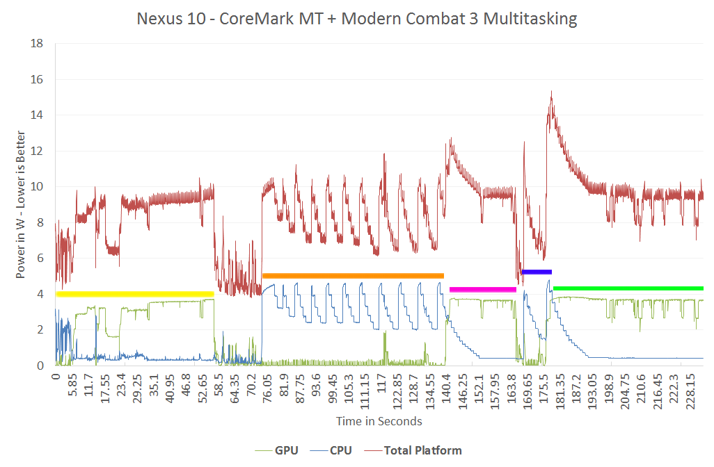
Throughout all of our Cortex A15 testing we kept bumping into that 4W ceiling with both the CPU and GPU - but we rarely saw both blocks use that much power at the same time. Intel actually tipped me off to this test to find out what happens if we try and force both the CPU and GPU to run at max performance at the same time. The graph below is divided into five distinct sections, denoted by colored bars above the sections. On this chart I have individual lines for GPU power consumption (green), CPU power consumption (blue) and total platform power consumption, including display, measured at the battery (red).
在整个A15的测试中,我们不断达到CPU和GPU分别的功率限制:4W,但是基本没有发生CPU和GPU同时达到这种功率的情况。实际上Intel悄悄的告诉我怎么搞这种测试,让GPU和CPU都同时达到最大功耗,看看将会发生什么。(话说Intel存心要坑Arm,呵呵)。下边的图总共分成五段,在上边有不同颜色的粗线标明。在图中分别有绿线表示GPU的功耗,蓝线表示CPU的功耗,用红线表示整个系统的功耗。
In the first section (yellow), we begin playing Modern Combat 3 - a GPU intensive first person shooter. GPU power consumption is just shy of 4W, while CPU power consumption remains below 1W. After about a minute of play we switch away from MC3 and you can see both CPU and GPU power consumption drop considerably. In the next section (orange), we fire up a multithreaded instance of CoreMark - a small CPU benchmark - and allow it to loop indefinitely. CPU power draw peaks at just over 4W, while GPU power consumption is understandably very low.
在第一段黄线,我们开了“现代战争3”,这是一个GPU敏感的第一人称设计游戏。这时候GPU的功耗飙到限制的4W,CPU功耗仍然保持1W。在游戏了1分钟之后,我们从现代战争中切换出来,可以看到CPU和GPU的功耗都明显下降了。在下一段,橙色表示,我们开了一个CoreMark多线程测试,这是一个小尺寸的设计,可以不断循环运行。CPU的功耗最大达到了4W,同时GPU的功耗很低。
Next, while CoreMark is still running on both cores, we switch back to Modern Combat 3 (pink section of the graph). GPU voltage ramps way up, power consumption is around 4W, but note what happens to CPU power consumption. The CPU cores step down to a much lower voltage/frequency for the background task (~800MHz from 1.7GHz). Total SoC TDP jumps above 4W but the power controller quickly responds by reducing CPU voltage/frequency in order to keep things under control at ~4W. To confirm that CoreMark is still running, we then switch back to the benchmark (blue segment) and you see CPU performance ramps up as GPU performance winds down. Finally we switch back to MC3, combined CPU + GPU power is around 8W for a short period of time before the CPU is throttled.
截下来,在CoreMark在两个CPU核心上运行的时候,我们切换到现代战争,如粉色所示。这时候GPU供电的电压猛增,功耗接近于4W,请注意CPU的功耗发生了什么。这时候CPU的电压和功率大幅度降低,从1.7G下降到800MHz。在切换的时候,总的Soc处理器的TDP超过了4W,但是电源控制单元迅速的反应,降低CPU的电压和频率,使得整个功耗得到控制,维持在4W左右。为了验证CoreMark还在运行,我们切换到该程序,蓝色所示,我们看到CPU性能猛增而GPU相应下降。最后我们切换回现代战争,在CPU降速之前,整个CPU和GPU的功耗达到了8W。
Now this is a fairy contrived scenario, but it's necessary to understand the behavior of the Exynos 5250. The SoC is allowed to reach 8W, making that its max TDP by conventional definitions, but seems to strive for around 4W as its typical power under load. Why are these two numbers important? With Haswell, Intel has demonstrated interest (and ability) to deliver a part with an 8W TDP. In practice, Intel would need to deliver about half that to really fit into a device like the Nexus 10 but all of the sudden it seems a lot more feasible. Samsung hits 4W by throttling its CPU cores when both the CPU and GPU subsystems are being taxed, I wonder what an 8W Haswell would look like in a similar situation...
尽管这是一个人为设计出来的场合,但是有必要里了解一下Exynos 5250的行为。这个Soc允许达到8W,按照传统的定义,这个就是其最大TDP,但是在运行中将努力将功耗控制在4W,作为典型的负载功耗。我为什么这两个数字这么重要?对于Haswell,Intel已经展示推出8W TDP型号的兴趣和能力。实际上,Intel要把他塞进Nexus 10这样的设备,需要再将这个功耗降低一半。但是经过上述测试,这种可能突然大增。三星在Soc达到4W的功耗限制的时候迫使CPU降压降频,我怀疑8W的Haswell也可以照此办理……
|
|


 IP卡
IP卡 狗仔卡
狗仔卡
 发表于 2013-1-5 01:27

 QQ好友和群
 收藏
收藏 分享
分享 好贴
好贴 烂贴
烂贴 提升卡
提升卡 置顶卡
置顶卡 沉默卡
沉默卡 喧嚣卡
喧嚣卡 变色卡
变色卡 显身卡
显身卡
